SLAAE45 September 2021 TMUXHS4412
2.4 Power and Grounding Layout Guidelines
- Use a complete ground plane and a
complete power plane to avoid noise coupling. But in most cases, split ground
planes cannot be avoided. If split ground planes are essential:
- Do not route signals over a gap. Always strive for the return current flow with the smallest loop area.
- Connect split ground planes only at one point. More common-ground connections can create ground loops, and this increases radiation.
- Power planes should only reference their own ground plane. They should not overlap with another ground plane.
- Do not connect bypass capacitors between a power plane and an unrelated ground plane. Again, noise can be coupled from one supply system into the other.
- Separate digital and analog power supplies with filtering and bypassing.
- Put the largest-value filter capacitors near a power connector and supply inputs.
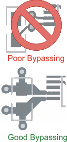
- Place high-quality X7R decoupling capacitors close to device pins.
- Use multiple capacitors (0.1 μF, 0.01 μF, and 1 μF) in parallel to offer low impedance over higher frequency ranges.
- Place the smallest-value capacitors closest to the power pin.
- Connect the pad of the capacitor directly to a via to the ground plane. Use two or three vias to get a low-impedance connection to ground.
- Keep the traces from decoupling caps to ground as short and wide as possible
 Figure 2-6 Poor and Good Placement and
Routing of Bypass Capacitors