SLAAE76B march 2023 – june 2023 MSPM0G1105 , MSPM0G1106 , MSPM0G1107 , MSPM0G1505 , MSPM0G1506 , MSPM0G1507 , MSPM0G3105 , MSPM0G3106 , MSPM0G3107 , MSPM0G3505 , MSPM0G3506 , MSPM0G3507
7.2 UART and LIN Resources and Design Considerations
The MSPM0G series MCU includes Universal Asynchronous Receiver-Transmitter (UART). As seen in Table 7-4, UART0 supports LIN, DALI, IrDA, ISO7816 Manchester Coding function.
| UART Features | UART0 (Extend) | UART1 (Main) |
|---|---|---|
| Active in Stop and Standby Mode | Yes | Yes |
| Separate transmit and receive FIFOs | Yes | Yes |
| Support hardware flow control | Yes | Yes |
| Support 9-bit configuration | Yes | Yes |
| Support LIN mode | Yes | - |
| Support DALI | Yes | - |
| Support IrDA | Yes | - |
| Support ISO7816 Smart Card | Yes | - |
| Support Manchester coding | Yes | - |
The MSPM0G UART module can support up to 10-MHz baud date in Power Domain1 to support almost all UART applications.
| PARAMETERS | TEST CONDITIONS | MIN | TYP | MAX | UNIT | |
|---|---|---|---|---|---|---|
| fUART | UART input clock frequency | UART in Power Domain1 | 80 | MHz | ||
| fUART | UART input clock frequency | UART in Power Domain0 | 40 | MHz | ||
| fBITCLK | BITCLK clock frequency(equals baud rate in MBaud) | UART in Power Domain1 | 10 | MHz | ||
| fBITCLK | BITCLK clock frequency(equals baud rate in MBaud) | 5 | MHz | |||
| tSP | Pulse duration of spikes suppressed by input filter | AGFSELx = 0 | 5 | 5.5 | 32 | ns |
| AGFSELx = 1 | 8 | 15 | 55 | ns | ||
| AGFSELx = 2 | 18 | 38 | 115 | ns | ||
| AGFSELx = 3 | 30 | 74 | 165 | ns | ||
Local Interconnect Network (LIN) is a commonly used low-speed network interface that consists of a commander node communicating with multiple remote responder nodes. Only a single wire is required for communication and is commonly included in the vehicle wiring harness.
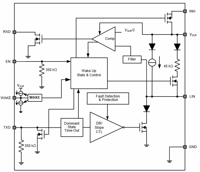
The TLIN1021A-Q1 transmitter supports data rates up to 20 kbps. The transceiver controls the state of the LIN bus via the TXD pin and reports the state of the bus on its open-drain RXD output pin. The device has a current-limited wave-shaping driver to reduce electromagnetic emissions (EME).
The TLIN1021A-Q1 is designed to support 12-V applications with a wide input voltage operating range. The device supports low-power sleep mode and wake-up from low-power mode over LIN, the WAKE pin, or the EN pin. The device allows for system-level reductions in battery current consumption by selectively enabling the various power supplies that can be present on a node through the TLIN1021A-Q1 INH output pin. Figure 7-1 shows a typical interface implemented using the TI TLIN1021A LIN transceiver.
 Figure 7-1 Typical LIN TLIN1021A Transceiver
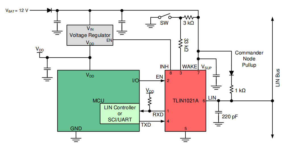
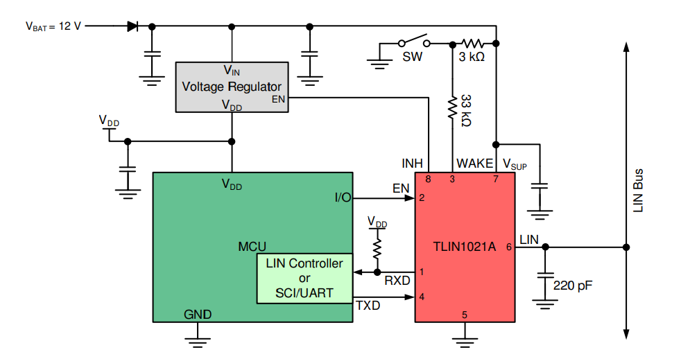
Only a single wire is required for communication and is commonly included in the vehicle wiring harness. Figure 7-2 and Figure 7-3 show typical interfaces implemented using the TI TLIN1021A LIN transceiver, for more details refer to the TLIN1021 data sheet.
 Figure 7-2 Typical LIN Application
(Commander) With MSPM0G
 Figure 7-3 Typical LIN Application
(Responder) With MSPM0G