SLAAEF9 November   2023 MSPM0L1306


  1.   1
  2.   Abstract
  3.   Trademarks
  4. 1MSPM0 Portfolio Overview
    1. 1.1 Introduction
    2. 1.2 Portfolio Comparison of Renesas RL78 MCUs to MSPM0 MCUs
  5. 2Ecosystem And Migration
    1. 2.1 Ecosystem Comparison
      1. 2.1.1 MSPM0 Software Development Kit (MSPM0 SDK)
      2. 2.1.2 The IDE Supported By MSPM0
      3. 2.1.3 SysConfig
      4. 2.1.4 Debug Tools
      5. 2.1.5 LaunchPad
    2. 2.2 Migration Process
      1. 2.2.1 Step 1. Choose The Right MSPM0 MCU
      2. 2.2.2 Step 2. Set Up IDE And Quick Introduction of CCS
        1. 2.2.2.1 Set Up IDE
        2. 2.2.2.2 Quick Introduction of CCS
      3. 2.2.3 Step 3. Set Up MSPM0 SDK And Quick Introduction of MSPM0 SDK
        1. 2.2.3.1 Set Up MSPM0 SDK
        2. 2.2.3.2 Quick Introduction of SDK
      4. 2.2.4 Step 4. Software Evaluation
      5. 2.2.5 Step 5. PCB Board Design
      6. 2.2.6 Step 6. Mass Production
    3. 2.3 Example
  6. 3Core Architecture Comparison
    1. 3.1 CPU
    2. 3.2 Embedded Memory Comparison
      1. 3.2.1 Flash Features
      2. 3.2.2 Flash Organization
        1. 3.2.2.1 Flash Memory Regions
        2. 3.2.2.2 NONMAIN Memory of MSPM0
        3. 3.2.2.3 Flash Memory Registers of RL78
      3. 3.2.3 Embedded SRAM
    3. 3.3 Power UP and Reset Summary and Comparison
    4. 3.4 Clocks Summary and Comparison
      1. 3.4.1 Oscillators
        1. 3.4.1.1 MSPM0 Oscillators
      2. 3.4.2 Clock Signal Comparison
    5. 3.5 MSPM0 Operating Modes Summary and Comparison
      1. 3.5.1 Operating Modes Comparison
      2. 3.5.2 MSPM0 Capabilities in Lower Modes
      3. 3.5.3 Entering Lower-Power Modes
      4. 3.5.4 Low-Power Mode Code Examples
    6. 3.6 Interrupts and Events Comparison
      1. 3.6.1 Interrupts and Exceptions
        1. 3.6.1.1 Interrupt Management of RL78
        2. 3.6.1.2 Interrupt Management of MSPM0
      2. 3.6.2 Event Handler of MSPM0
      3. 3.6.3 Event Link Controller (ELC) of RL78
      4. 3.6.4 Event Management Comparison
    7. 3.7 Debug and Programming Comparison
      1. 3.7.1 Debug Comparison
      2. 3.7.2 Programming Mode Comparison
        1. 3.7.2.1 Bootstrap Loader (BSL) Programming of MSPM0
        2. 3.7.2.2 Serial Programming (Using External Device) of RL78
  7. 4Digital Peripheral Comparison
    1. 4.1 General-Purpose I/O (GPIO, IOMUX)
    2. 4.2 Universal Asynchronous Receiver-Transmitter (UART)
    3. 4.3 Serial Peripheral Interface (SPI)
    4. 4.4 Inter-Integrated Circuit (I2C)
    5. 4.5 Timers (TIMGx, TIMAx)
    6. 4.6 Windowed Watchdog Timer (WWDT)
    7. 4.7 Real-Time Clock (RTC)
  8. 5Analog Peripheral Comparison
    1. 5.1 Analog-to-Digital Converter (ADC)
    2. 5.2 Comparator (COMP)
    3. 5.3 Digital-to-Analog Converter (DAC)
    4. 5.4 Operational Amplifier (OPA)
    5. 5.5 Voltage References (VREF)

Interrupt Management of MSPM0

Unlike RL78 devices, MSPM0 devices set the priority level of each peripheral interrupt source through the IPRx registers in the NVIC, and mask/unmask a peripheral interrupt source through ISER and ICER register in the NVIC. Each peripheral interrupt contains kinds of interrupt conditions. For example, as a peripheral interrupt source, UARTx has multiple interrupt conditions such as transmit interrupt and receive interrupt, and so forth. And the interrupt conditions are managed by six standard registers in the peripheral side.

Figure 3-3 shows the peripheral interrupt hierarchy.
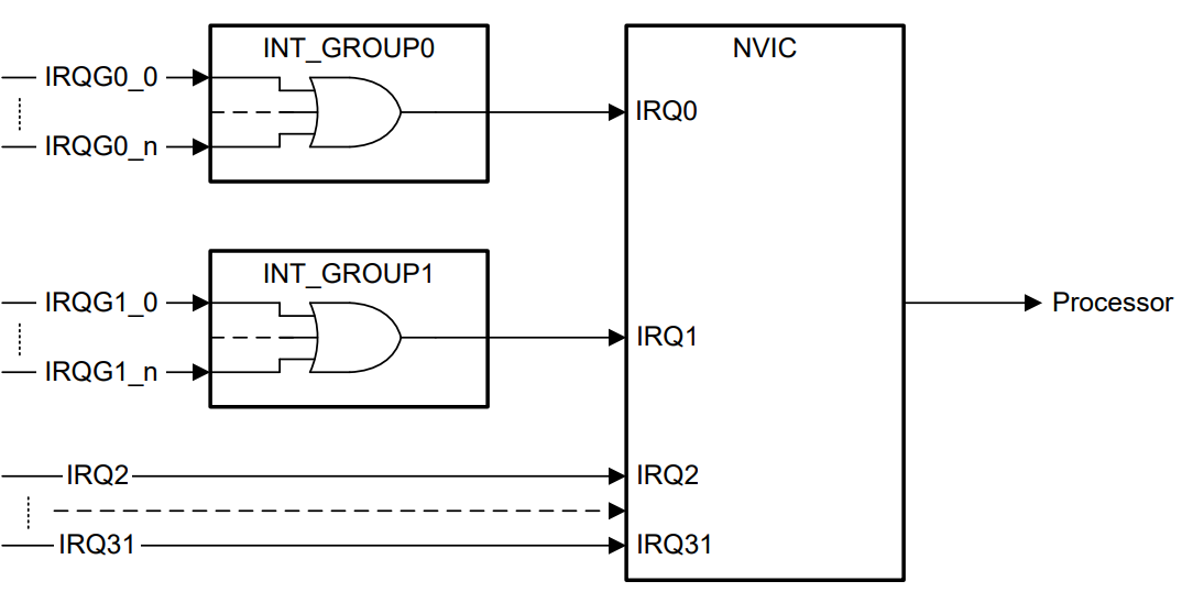
GUID-490A3085-9F46-4357-A5ED-282CAFE0E749-low.png Figure 3-3 Peripheral Interrupt Hierarchy of MSPM0