SLAZ146I October   2012  – May 2021 MSP430F1611


  1. 1Functional Advisories
  2. 2Preprogrammed Software Advisories
  3. 3Debug Only Advisories
  4. 4Fixed by Compiler Advisories
  5. 5Nomenclature, Package Symbolization, and Revision Identification
    1. 5.1 Device Nomenclature
    2. 5.2 Package Markings
      1.      RTD64
      2.      PM64
    3. 5.3 Memory-Mapped Hardware Revision (TLV Structure)
  6. 6Advisory Descriptions
    1. 6.1  ADC18
    2. 6.2  ADC25
    3. 6.3  BCL5
    4. 6.4  CPU4
    5. 6.5  CPU41
    6. 6.6  DAC4
    7. 6.7  I2C7
    8. 6.8  I2C8
    9. 6.9  I2C9
    10. 6.10 I2C10
    11. 6.11 I2C11
    12. 6.12 I2C12
    13. 6.13 I2C13
    14. 6.14 I2C14
    15. 6.15 I2C15
    16. 6.16 I2C16
    17. 6.17 MPY2
    18. 6.18 TA12
    19. 6.19 TA16
    20. 6.20 TA21
    21. 6.21 TAB22
    22. 6.22 TB2
    23. 6.23 TB16
    24. 6.24 TB24
    25. 6.25 US14
    26. 6.26 US15
    27. 6.27 WDG2
  7. 7Revision History

MPY2

MPY Module

Category

Functional

Function

Multiplier Result register corruption

Description

Depending on the address of the write instruction, writing to the multiplier result registers (RESHI, RESLO, or SUMEXT) may corrupt the result registers. The address dependency varies between a 2-word and a 3-word instructions.

Workaround

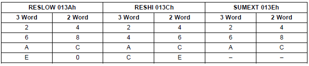
Ensure that a write instruction to an MPY result register (for example, mov.w #200, &RESHI) is not located at an address with the four least significant bits shown in Table 1:

Table 1. Sensitive Addresses for Write Access to MPY Result Registers MAB[3:0]


GUID-20201119-CA0I-10CF-JKCX-GW97CVV86PDZ-low.png