SLLSEH0F July 2013 – August 2014 SN65HVD01
PRODUCTION DATA.
- 1 Features
- 2 Applications
- 3 Description
- 4 Revision History
- 5 Pin Configuration and Functions
- 6 Specifications
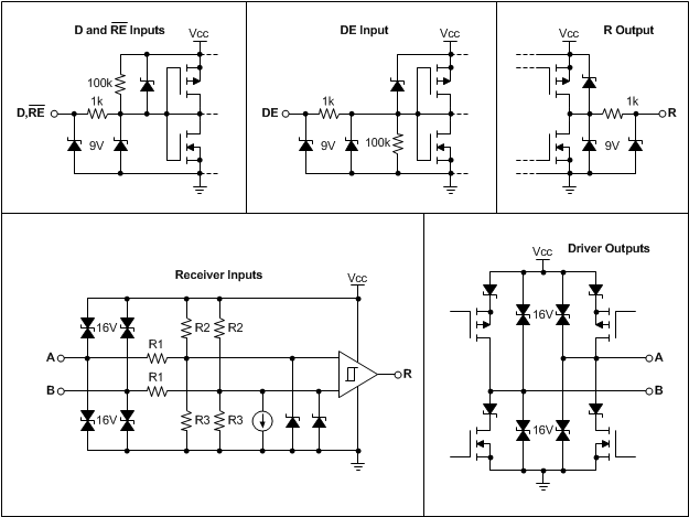
- 7 Parameter Measurement Information
- 8 Detailed Description
- 9 Applications and Implementation
- 10Power Supply Recommendations
- 11Layout
- 12Device and Documentation Support
- 13Mechanical, Packaging, and Orderable Information
8 Detailed Description
8.1 Overview
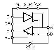
The SN65HVD01 is a low-power, half-duplex RS-485 transceiver whose maximum data rate can be set to either 250 kbps or 20 Mbps via a selection terminal, SLR.
The device possesses two power supply inputs, one for logic control functions, VL, and the other for the bus supply, VCC. VL can range from 1.65 V minimum up to 3.6 V maximum and allows for the direct interface to low-voltage FPGAs and micro controllers. VCC requires a supply between 3 V to 3.6 V to assure sufficient output drive capability across a wide common-mode range.
8.2 Functional Block Diagram
8.3 Feature Description
Internal ESD protection circuits protect the transceiver against Electrostatic discharges (ESD) according to IEC61000-4-2 of up to ±16 kV, and against electrical fast transients (EFT) according to IEC61000-4-4 of up to ±4 kV.
The SN65HVD01 provides internal biasing of the receiver input thresholds in combination with large input-threshold hysteresis. At a positive input threshold of VIT+ = –60 mV and an input hysteresis of VHYS = 70 mV, the receiver output remains logic high even in the presence of 130 mVPK differential noise without the need for external failsafe biasing resistors.
Device operation is specified over a wide temperature range from –40°C to 125°C.
8.4 Device Functional Modes
When driver enable terminal, DE, is logic high, the differential outputs A and B follow the logic states at data input D. A logic high at D causes A to turn high and B to turn low. In this case the differential output voltage defined as VOD = VA – VB is positive. When D is low, the output states reverse, B turns high, A becomes low, and VOD is negative.
When DE is low, both outputs turn high-impedance. In this condition, the logic state at D is irrelevant. The DE terminal has an internal pull-down resistor to ground, thus when left open the driver is disabled (high-impedance) by default. The D terminal has an internal pull-up resistor to VL, thus, when left open while the driver is enabled, output A turns high and B turns low.
Table 1. Driver Function Table
| INPUT | ENABLE | OUTPUTS | FUNCTION | |
|---|---|---|---|---|
| D | DE | A | B | |
| H | H | H | L | Actively drive bus High |
| L | H | L | H | Actively drive bus Low |
| X | L | Z | Z | Driver disabled |
| X | OPEN | Z | Z | Driver disabled by default |
| OPEN | H | H | L | Actively drive bus High by default |
When the receiver enable terminal, RE, is logic low, the receiver is enabled. When the differential input voltage defined as VID = VA – VB is positive and higher than the positive input threshold, VIT+, the receiver output, R, turns high. When VID is negative and less than the negative and lower than the negative input threshold, VIT-, the receiver output, R, turns low. If VID is between VIT+ and VIT- the output is indeterminate.
When RE is logic high or left open, the receiver output is high-impedance and the magnitude and polarity of VID are irrelevant. Internal biasing of the receiver inputs causes the output to go failsafe-high when the transceiver is disconnected from the bus (open-circuit), the bus lines are shorted (short-circuit), or the bus is not actively driven (idle bus).
Table 2. Receiver Function Table
| DIFFERENTIAL INPUT | ENABLE | OUTPUT | FUNCTION |
|---|---|---|---|
| VID = VA – VB | RE | R | |
| VIT+ < VID | L | H | Receive valid bus High |
| VIT– < VID < VIT+ | L | ? | Indeterminate bus state |
| VID < VIT– | L | L | Receive valid bus Low |
| X | H | Z | Receiver disabled |
| X | OPEN | Z | Receiver disabled by default |
| Open-circuit bus | L | H | Fail-safe high output |
| Short-circuit bus | L | H | Fail-safe high output |
| Idle (terminated) bus | L | H | Fail-safe high output |
Connecting SLR to VL limits the maximum data rate to 250 kbps and increases the driver rise and fall times to 800 ns. Connecting SLR to GND increases the upper data rate limit to 20 Mbps and reduces the driver rise and fall times to 10 ns.
Table 3. SLR-Terminal Configuration
| SLR-INPUT | DATA RATE | TYP tr / tf |
|---|---|---|
| VL | 250 kbps | 800 ns |
| GND or OPEN | 20 Mbps | 10 ns |