SLLSEH0F July 2013 – August 2014 SN65HVD01
PRODUCTION DATA.
- 1 Features
- 2 Applications
- 3 Description
- 4 Revision History
- 5 Pin Configuration and Functions
- 6 Specifications
- 7 Parameter Measurement Information
- 8 Detailed Description
- 9 Applications and Implementation
- 10Power Supply Recommendations
- 11Layout
- 12Device and Documentation Support
- 13Mechanical, Packaging, and Orderable Information
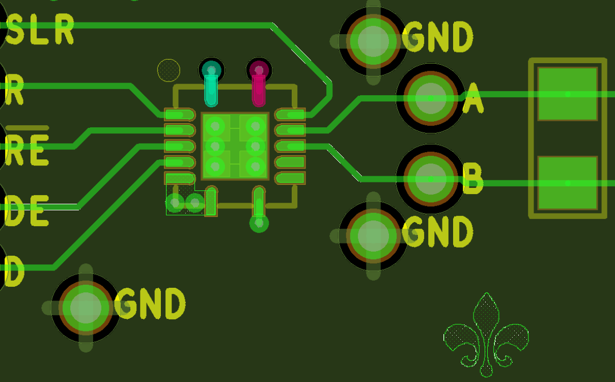
11 Layout
On-chip IEC-ESD protection is good for laboratory and portable equipment but never sufficient for EFT and surge transients occurring in industrial environments. Therefore robust and reliable bus node design requires the use of external transient protection devices.
Because ESD and EFT transients have a wide frequency bandwidth from approximately 3 MHz to 3 GHz, high-frequency layout techniques must be applied during PCB design.
In order for your PCB design to be successful start with the design of the protection circuit in mind.
11.1 Layout Guidelines
- Place the protection circuitry close to the bus connector to prevent noise transients from penetrating your board.
- Use VCC and ground planes to provide low-inductance. Note that high-frequency currents follow the path of least inductance and not the path of least impedance.
- Design the protection components into the direction of the signal path. Do not force the transients currents to divert from the signal path to reach the protection device.
- Apply 100 nF to 220 nF bypass capacitors as close as possible to the VCC terminals of transceiver, UART, controller ICs on the board.
- Use at least two vias for VCC and ground connections of bypass capacitors and protection devices to minimize effective via-inductance.
- Use 1k to 10k pull-up/down resistors for enable lines to limit noise currents in theses lines during transient events.
- Insert pulse-proof resistors into the A and B bus lines if the TVS clamping voltage is higher than the specified maximum voltage of the transceiver bus terminals. These resistors limit the residual clamping current into the transceiver and prevent it from latching up.
- While pure TVS protection is sufficient for surge transients up to 1kV, higher transients require metal-oxide varistors (MOVs) which reduce the transients to a few hundred volts of clamping voltage, and transient blocking units (TBUs) that limit transient current to less than 1 mA.
11.2 Layout Example