SLLSEY6G October 2017 – February 2024 TLIN2029-Q1
PRODUCTION DATA
- 1
- 1 Features
- 2 Applications
- 3 Description
- 4 Pin Configuration and Functions
- 5 Specifications
- 6 Parameter Measurement Information
-
7 Detailed Description
- 7.1 Overview
- 7.2 Functional Block Diagram
- 7.3
Feature Description
- 7.3.1 LIN (Local Interconnect Network) Bus
- 7.3.2 TXD (Transmit Input and Output)
- 7.3.3 RXD (Receive Output)
- 7.3.4 VSUP (Supply Voltage)
- 7.3.5 GND (Ground)
- 7.3.6 EN (Enable Input)
- 7.3.7 Protection Features
- 7.3.8 TXD Dominant Time Out (DTO)
- 7.3.9 Bus Stuck Dominant System Fault: False Wake-Up Lockout
- 7.3.10 Thermal Shutdown
- 7.3.11 Under Voltage on VSUP
- 7.3.12 Unpowered Device and LIN Bus
- 7.4 Device Functional Modes
- 8 Application and Implementation
- 9 Device and Documentation Support
- 10Revision History
- 11Mechanical, Packaging, and Orderable Information
6 Parameter Measurement Information
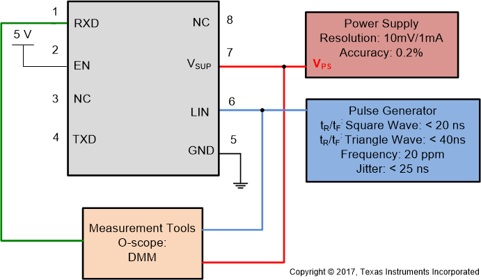 Figure 6-1 Test System: Operating Voltage Range with RX and TX Access: Parameters 9, 10
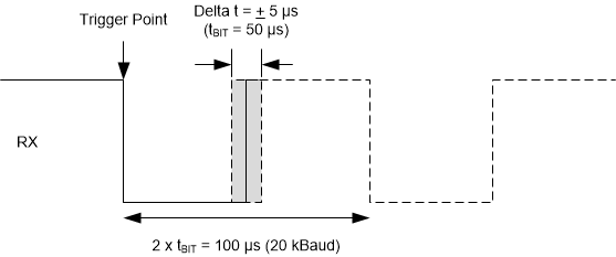 Figure 6-2 RX Response: Operating Voltage Range
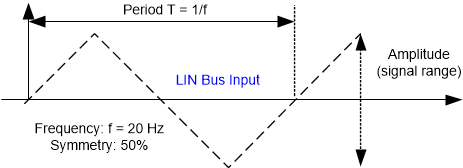 Figure 6-3 LIN Bus Input Signal
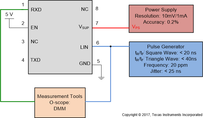 Figure 6-4 LIN Receiver Test with RX access Param 17, 18, 19, 20
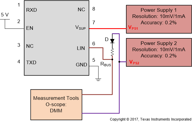 Figure 6-5 VSUP_NON_OP Param 1154/56
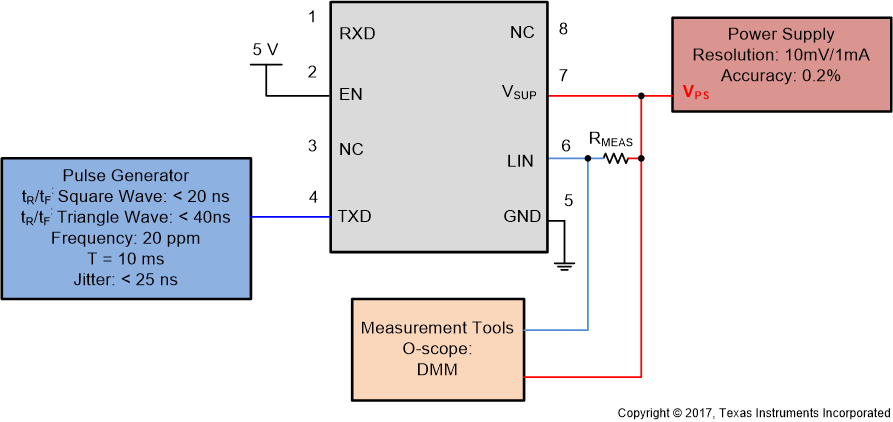 Figure 6-6 Test Circuit for IBUS_LIM at Dominant State (Driver on) Param 12
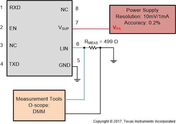 Figure 6-7 Test Circuit for IBUS_PAS_dom; TXD = Recessive State VBUS = 0 V, Param 13
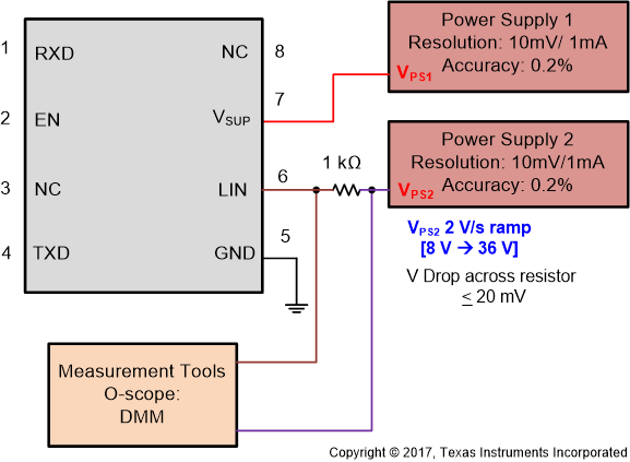 Figure 6-8 Test Circuit for IBUS_PAS_rec Param 14
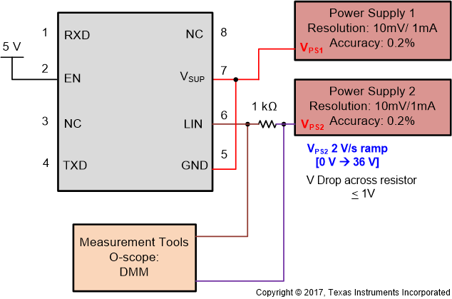 Figure 6-9 Test Circuit for IBUS_NO_GND Loss of GND
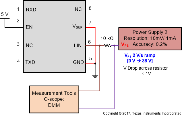 Figure 6-10 Test Circuit for IBUS_NO_BAT Loss of Battery
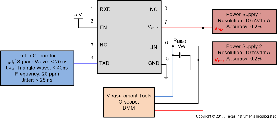 Figure 6-11 Test Circuit Slope Control and Duty Cycle Param 27, 28, 29, 30, 72, 73, 74, 75
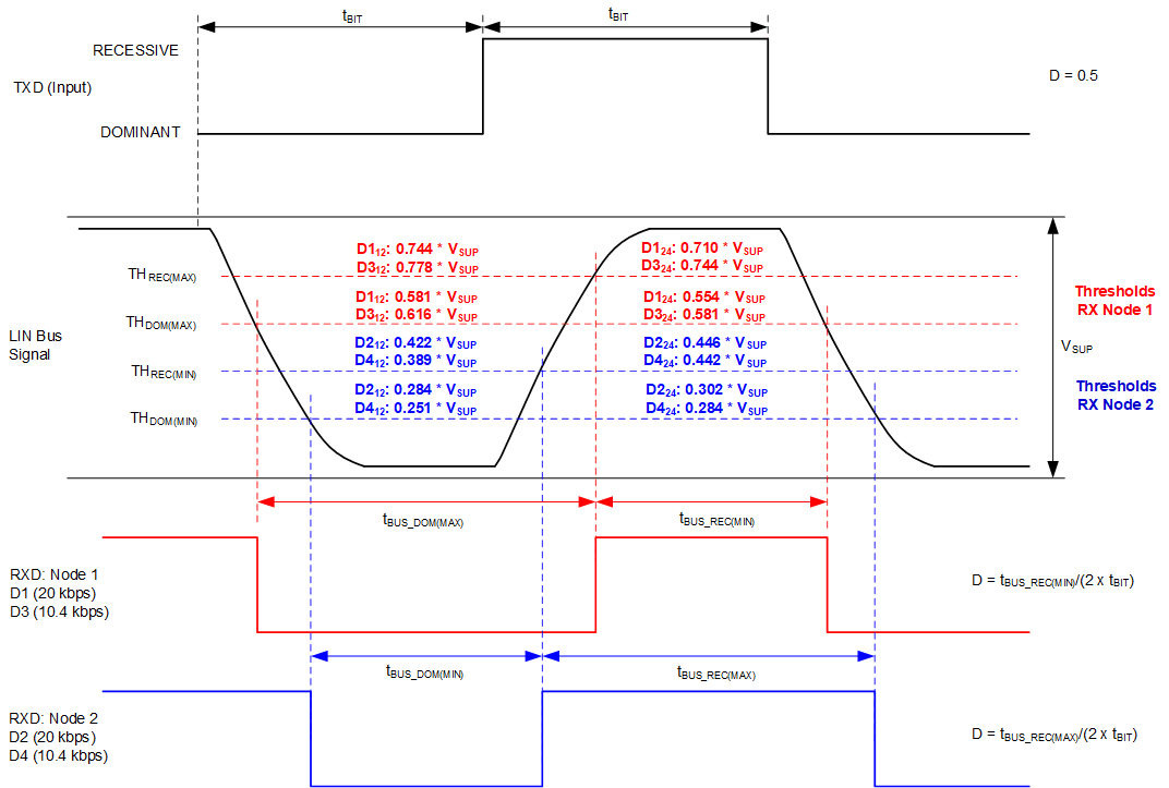 Figure 6-12 Definition of Bus Timing Parameters
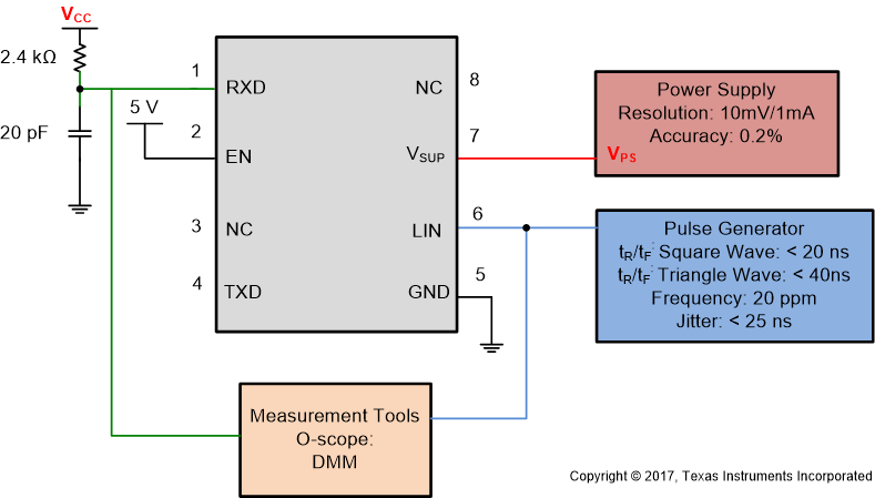 Figure 6-13 Propagation Delay Test Circuit; Param 31, 32
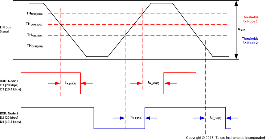 Figure 6-14 Propagation Delay
 Figure 6-15 Mode Transitions
 Figure 6-16 Wake-up Through EN
 Figure 6-17 Wake-up through LIN
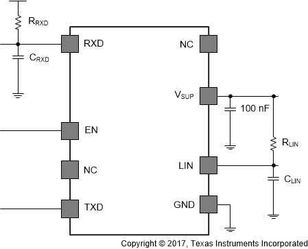 Figure 6-18 Test Circuit for AC Characteristics