SLLU173C October 2012 – September 2021 SN65176B , SN65HVD05 , SN65HVD06 , SN65HVD07 , SN65HVD08 , SN65HVD10 , SN65HVD11 , SN65HVD1176 , SN65HVD12 , SN65HVD1780 , SN65HVD1781 , SN65HVD1782 , SN65HVD1785 , SN65HVD1786 , SN65HVD1787 , SN65HVD1794 , SN65HVD20 , SN65HVD21 , SN65HVD22 , SN65HVD23 , SN65HVD24 , SN65HVD3082E , SN65HVD3085E , SN65HVD3088E , SN65HVD485E , SN65HVD72 , SN65HVD75 , SN65HVD78 , SN65HVD82 , SN65LBC176 , SN65LBC176A , SN65LBC182 , THVD1419 , THVD1429
3 EVM Setup and Precautions
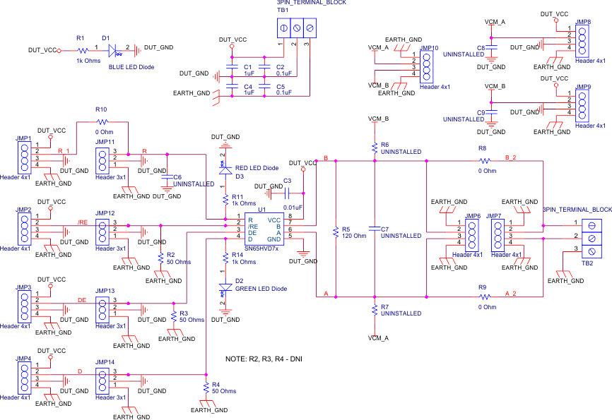
Figure 3-1 shows the schematic of the EVM. The EVM board has headers labeled from JMP1 to JMP14 (JMP5 is omitted) and two 3-pin terminal blocks labeled TB1 and TB2. These headers support device evaluation for a wide range of system configurations.
The examples in this document show a 3.3-V signal generator and a 3.3-V power supply unit. Depending on the Texas Instruments RS-485 device chosen, the user may need to provide a 5-V signal generator input and 5-V power supply.
- Pin 1 (EARTH) is a second ground pin that allows applying an external voltage between GND and EARTH to simulate common-mode voltage conditions.
- Pin 2 (GND) is connected to the negative output or ground terminal of the PSU. This pin represents the ground potential of the device-under-test and the entire EVM. It also connects to various jumpers on the board.
- Pin 3 (VCC) is connected to the positive output of a regulated power supply unit (PSU) as it represents the positive supply voltage of the device-under-test and also connects to various jumpers on the board.
 Figure 3-1 RS-485 Half-Duplex EVM Schematic
For the first measurements, ignore the common-mode simulation and connect EARTH to GND through a wire-bridge between pin 1 and pin 2 of TB1.
 Figure 3-2 Bridging DUT_GND with EARTH_GND
While JMP2 to JMP4 are stimulation points, or headers through which the control and data signals for the RS485 Half-Duplex EVM are applied, JMP1, and JMP11 to JMP14 are probe points, or headers at which these signal can be measured.
Note that the 50-Ω resistors, R2, R3, and R4, have the index n.a., indicating that these components are not assembled. Because signal generators have a typical source impedance of 50 Ω, their output signal is twice the required signal voltage, and assumes that the on-board 50-Ω resistors divide this voltage down to the correct signal level.
Without these resistors; however, this voltage divider action is not accomplished, and the generator output voltage must be reduced to match the VCC requirements of the RS-485 device.
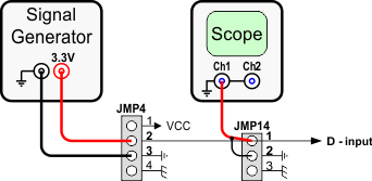
 Figure 3-3 Example for Stimulus and Probe Points with JMP4 and JMP14
Figure 3-3 gives an example for entering a data signal into the driver section of the transceiver. The signal output of the generator is adjusted to match the device VCC power supply requirements . The generator’s ground terminal is connected with pin 3, and the signal output terminal with pin 2 of JMP4. The data signal is measured through an oscilloscope with its signal input connected to pin 1 and its ground wire connected to pin 2 of JMP14.
The same setup applies to the DE and RE inputs through their corresponding headers JMP2 and JMP12 and JMP3 and JMP13. JMP1 however, must not receive a signal stimulus. Like JMP11, it represents the receiver output, R, of the half-duplex RS-485 device.
Instead of using signal generators, the EVM can directly interface to the micro controller I/O. Then the non-assembled 50-Ω resistors are of no concern. However, for proper operation, it must be assured that the high-level input voltage VIH ≥ 2 V and the low-level input voltage VIL ≤ 0.8 V.