SLLU173C October 2012 – September 2021 SN65176B , SN65HVD05 , SN65HVD06 , SN65HVD07 , SN65HVD08 , SN65HVD10 , SN65HVD11 , SN65HVD1176 , SN65HVD12 , SN65HVD1780 , SN65HVD1781 , SN65HVD1782 , SN65HVD1785 , SN65HVD1786 , SN65HVD1787 , SN65HVD1794 , SN65HVD20 , SN65HVD21 , SN65HVD22 , SN65HVD23 , SN65HVD24 , SN65HVD3082E , SN65HVD3085E , SN65HVD3088E , SN65HVD485E , SN65HVD72 , SN65HVD75 , SN65HVD78 , SN65HVD82 , SN65LBC176 , SN65LBC176A , SN65LBC182 , THVD1419 , THVD1429
2 Overview
TI RS-485 half-duplex devices in the 8-pin SOIC package have robust drivers and receivers in a small package for demanding industrial applications. The bus pins are robust to ESD events, with high levels of protection to Human-Body Model and IEC Contact Discharge specifications. These devices each combine a differential driver and a differential receiver, which operate from a single power supply. The driver differential outputs and the receiver differential inputs are connected internally to form a bus port suitable for half-duplex (two-wire bus) communication, and all feature a wide common-mode voltage range making the devices suitable for multi-point applications over long cable runs. TI's RS-485 devices are characterized for industrial applications.
This EVM comes without a transceiver soldered on to the board. The user can order any TI half-duplex, 8-pin SOIC RS-485 transceiver and solder it down on the board for evaluation. The EVM Tools Folder contains links to devices that work with this EVM. See http://www.ti.com/tool/rs485-hf-dplx-evm for more information.
Using the SN65HVD888 with Bus Polarity Correction Feature
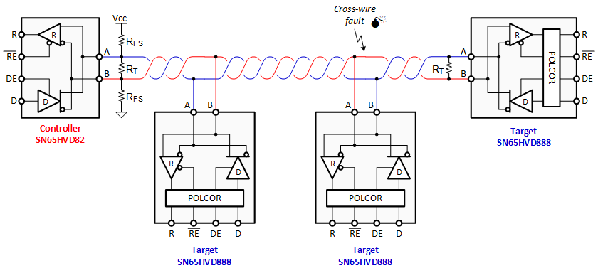
This EVM can support the SN65HVD888 half-duplex RS-485 transceiver with bus polarity correction (See Figure 2-1). The SN65HVD888 transceiver corrects a wrong bus signal polarity caused by a cross-wire fault. In order to detect the bus polarity all three of the following conditions must be met:
- a failsafe biasing network must be implemented (at the controller node) to set logic reference and define the signal polarity of the bus,
- a target node must have its receiver enabled and its driver disabled ( RE = DE = Low),
- the bus must be idling for the failsafe time, tFS-max.
After the failsafe time has passed, the polarity correction is complete and is applied to both, receive and transmit channels. The status of the bus polarity is latched within the transceiver and maintained for subsequent data transmissions.
Note: Data streams of consecutive 0’s or 1’s with durations exceeding tFS-min can accidently trigger a wrong polarity correction and must be avoided.
 Figure 2-1 Typical Applications Diagram