SLLU339 July 2021 ISOW7740 , ISOW7741 , ISOW7742 , ISOW7743 , ISOW7744
6 PCB Layout and 3D Diagram
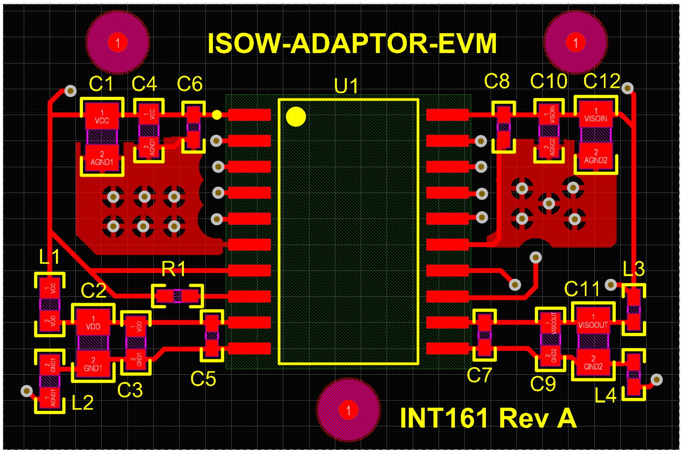
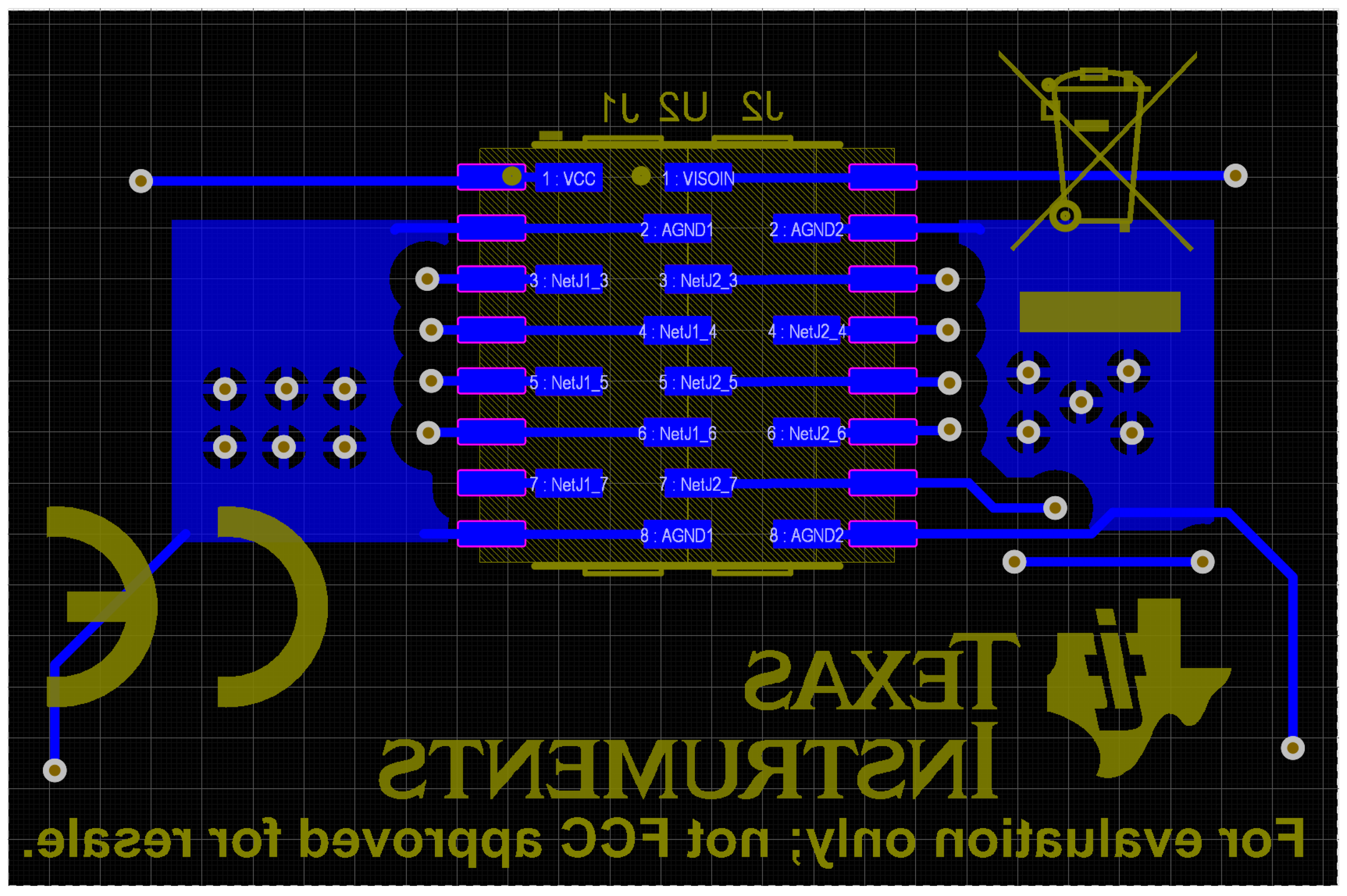
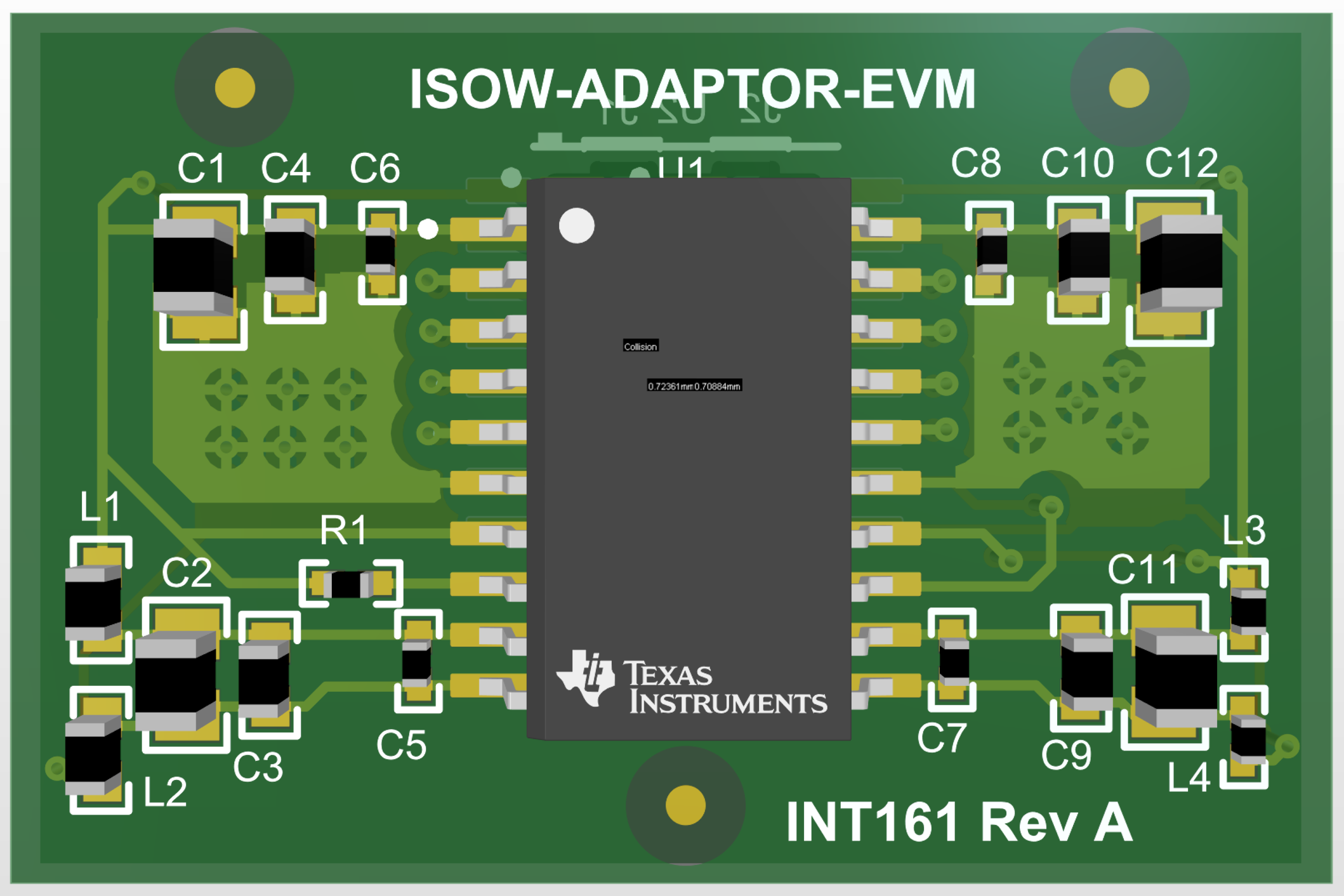
Figure 6-1 and Figure 6-2 show the printed-circuit board (PCB) layout top and bottom layers of the EVM, respectively, and Figure 6-3 shows a 3D diagram of the PCB visulizing how a finished board will look.
 Figure 6-1 ISOW-ADAPTOR-EVM PCB Layout -
Top Layer.
  Figure 6-2 ISOW-ADAPTOR-EVM PCB Layout -
Bottom Layer.
  Figure 6-3 ISOW-ADAPTOR-EVM PCB 3D
Diagram.