SLOA140B April 2009 – November 2018 TRF7960 , TRF7960A , TRF7961 , TRF7962A , TRF7963A
1.1 SCLK Polarity Switch
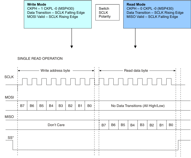
The SPI read operation is shown in Figure 2 below.
 Figure 2. Serial - SPI Interface Communication (Read Mode)
 The read command is sent out on the MOSI pin, MSB first in the first 8 clock cycles. MOSI data changes on the falling edge, and is validated in the reader on the rising edge (see Figure 2). During the write cycle the serial data out (MISO) is not valid. After the last read command bit (B0) is validated at the 8th rising edge of SCLK, after half a clock cycle, valid data can be read on the MISO pin at the falling edge of SCLK. It takes 8 clock edges to read out the full byte (MSB first).
NOTE
When using the hardware SPI (for example, a MSP430 hardware SPI) to implement the above feature, care must be taken to switch the SCLK polarity after write phase for proper read operation. The example clock polarity for the MSP430-specific environment is shown in the box above. Refer to the USARTSPI chapter for any specific microcontroller family for further information on the setting the appropriate clock polarity.
This clock polarity switch NEEDS to be done for all read (single, continuous) operations.
The MOSI (serial data out) should not have any transitions (all high or all low) during the read cycle. Also, the SS* should be low during the whole write and read operation.
The clock polarity switch is illustrated by the following pseudo code. This code refers specifically to the MSP430 platform. See the data sheet of the relevant microcontroller for your design.
   *pbuf = (0x40 | *pbuf);        // address, read, single
   *pbuf = (0x5f &*pbuf);         // register address
   while (!(IFG2 & UCB0TXIFG));   // USCI_B0 TX buffer ready?
   UCB0TXBUF = *pbuf;             // Previous data to TX, RX
   //while (!(IFG2 & UCB0RXIFG));
   temp=UCB0RXBUF;
   UCB0CTL1 |= UCSWRST;
   UCB0CTL0 &= ~UCCKPH;	      // switch clock polarity for read
   UCB0CTL1 &= ~UCSWRST;

   SPIStartCondition();           // SCLK High/Low to complete the cycle
   P3SEL |= BIT3;
   while (!(IFG2 & UCB0TXIFG));   // USCI_B0 TX buffer ready?
   UCB0TXBUF = 0x00;              // Receive initiated by a dummy TX write???

   while (!(IFG2 & UCB0RXIFG));
   _NOP();
   _NOP();
   *pbuf = UCB0RXBUF;
   pbuf++;
   lenght--;
   UCB0CTL0 |= UCCKPH;        // revert to original clock polarity
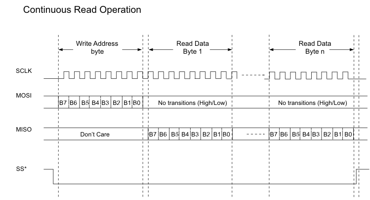
Figure 3 shows the continuous read operation.
 Figure 3. SPI Interface Communication (Continuous Read Mode)