SLOS626B December 2009 – November 2015 TPA2011D1
PRODUCTION DATA.
- 1 Features
- 2 Applications
- 3 Description
- 4 Revision History
- 5 Device Comparison Table
- 6 Pin Configuration and Functions
- 7 Specifications
- 8 Parameter Measurement Information
- 9 Detailed Description
- 10Application and Implementation
- 11Power Supply Recommendations
- 12Layout
- 13Device and Documentation Support
- 14Mechanical, Packaging, and Orderable Information
10 Application and Implementation
NOTE
Information in the following applications sections is not part of the TI component specification, and TI does not warrant its accuracy or completeness. TI’s customers are responsible for determining suitability of components for their purposes. Customers should validate and test their design implementation to confirm system functionality.
10.1 Application Information
These typical connection diagrams highlight the required external components and system level connections for proper operation of the device in several popular use cases. Each of these configurations can be realized using the Evaluation Modules (EVMs) for the device. These flexible modules allow full evaluation of the device in the most common modes of operation. Any design variation can be supported by TI through schematic and layout reviews. Visit e2e.ti.com for design assistance and join the audio amplifier discussion forum for additional information.
10.2 Typical Applications
10.2.1 TPA2011D1 with Differential Input
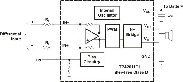
 Figure 33. Typical TPA2011D1 Application Schematic with Differential Input
10.2.1.1 Design Requirements
For this design example, use the parameters listed in Table 1.
Table 1. Design Parameters
| DESIGN PARAMETER | EXMAPLE VALUE |
|---|---|
| Power supply | 5 V |
| Enable input | High > 2 V |
| Low < 0.8 V | |
| Speaker | 8 Ω |
10.2.1.2 Detailed Design Procedure
10.2.1.2.1 Input Resistors (RI)
The input resistors (RI) set the gain of the amplifier according to the following equation.

Resistor matching is very important in fully differential amplifiers. The balance of the output on the reference voltage depends on matched ratios of the resistors. CMRR, PSRR, and cancellation of the second harmonic distortion diminish if resistor mismatch occurs. Therefore, it is recommended to use 1% tolerance resistors or better to keep the performance optimized. Matching is more important than overall tolerance. Resistor arrays with 1% matching can be used with a tolerance greater than 1%.
Place the input resistors very close to the TPA2011D1 to limit noise injection on the high-impedance nodes.
For optimal performance, the gain should be set to 2 V/V or lower. Lower gain allows the TPA2011D1 to operate at its best, and keeps a high voltage at the input making the inputs less susceptible to noise.
10.2.1.2.2 Decoupling Capacitor (CS)
The TPA2011D1 is a high-performance class-D audio amplifier that requires adequate power supply decoupling to ensure the efficiency is high and total harmonic distortion (THD) is low. For higher frequency transients, spikes, or digital hash on the line, a good low equivalent-series-resistance (ESR) ceramic capacitor, typically 1 μF, placed as close as possible to the device VDD lead works best. Placing this decoupling capacitor close to the TPA2011D1 is very important for the efficiency of the class-D amplifier, because any resistance or inductance in the trace between the device and the capacitor can cause a loss in efficiency. For filtering lower-frequency noise signals, a 10 μF or greater capacitor placed near the audio power amplifier would also help, but it is not required in most applications because of the high PSRR of this device.
10.2.2 TPA2011D1 with Differential Input and Input Capacitors
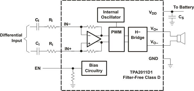
 Figure 34. TPA2011D1 Application Schematic with Differential Input and Input Capacitors
10.2.2.1 Design Requirements
For this design example, use the parameters listed in Table 1.
10.2.2.2 Detailed Design Procedure
For the design procedure see Input Resistors (RI) and Decoupling Capacitor (CS).
10.2.2.2.1 Input Capacitors (CI)
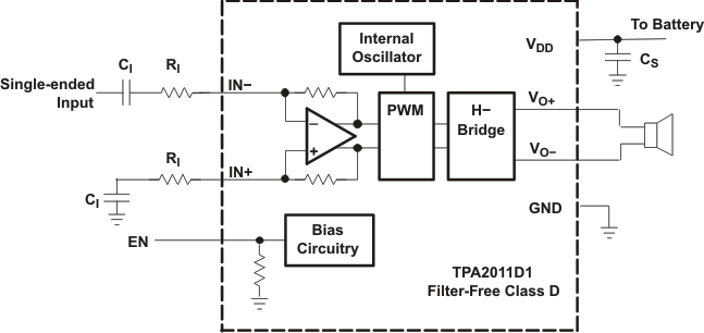
The TPA2011D1 does not require input coupling capacitors if the design uses a differential source that is biased from 0.5 V to VDD –0.8 V. If the input signal is not biased within the recommended common mode input range, if needing to use the input as a high pass filter, or if using a single-ended source, input coupling capacitors are required.
The input capacitors and input resistors form a high-pass filter with the corner frequency, fC, determined in the following equation.

The value of the input capacitor is important to consider as it directly affects the bass (low frequency) performance of the circuit. Speakers in wireless phones cannot usually respond well to low frequencies, so the corner frequency can be set to block low frequencies in this application.
The equation below is reconfigured to solve for the input coupling capacitance.

If the corner frequency is within the audio band, the capacitors should have a tolerance of ±10% or better, because any mismatch in capacitance causes an impedance mismatch at the corner frequency and below.
For a flat low-frequency response, use large input coupling capacitors (1 μF). However, in a GSM phone the ground signal is fluctuating at 217 Hz, but the signal from the codec does not have the same 217 Hz fluctuation. The difference between the two signals is amplified, sent to the speaker, and heard as a 217 Hz hum.
10.2.2.3 Application Curves
For application curves, see the figures listed in Table 2.
10.2.3 TPA2011D1 with Single-Ended Input
 Figure 35. TPA2011D1 Application Schematic with Single-Ended Input
10.2.3.1 Design Requirements
For this design example, use the parameters listed in Table 1.
10.2.3.2 Detailed Design Procedure
For the design procedure see Input Resistors (RI), Decoupling Capacitor (CS), and Input Capacitors (CI).
10.2.3.3 Application Curves
For application curves, see the figures listed in Table 2.