SLOS626B December   2009  – November 2015 TPA2011D1

PRODUCTION DATA.  

  1. Features
  2. Applications
  3. Description
  4. Revision History
  5. Device Comparison Table
  6. Pin Configuration and Functions
  7. Specifications
    1. 7.1 Absolute Maximum Ratings
    2. 7.2 ESD Ratings
    3. 7.3 Recommended Operating Conditions
    4. 7.4 Thermal Information
    5. 7.5 Electrical Characteristics
    6. 7.6 Operating Characteristics
    7. 7.7 Dissipation Ratings
    8. 7.8 Typical Characteristics
  8. Parameter Measurement Information
  9. Detailed Description
    1. 9.1 Overview
    2. 9.2 Functional Block Diagram
    3. 9.3 Feature Description
      1. 9.3.1 Fully Differential Amplifier
        1. 9.3.1.1 Advantages of Fully Differential Amplifiers
      2. 9.3.2 Eliminating the Output Filter With the TPA2011D1
        1. 9.3.2.1 Effect on Audio
        2. 9.3.2.2 When to Use an Output Filter
      3. 9.3.3 Short Circuit Auto-Recovery
      4. 9.3.4 Integrated Image Reject Filter for DAC Noise Rejection
    4. 9.4 Device Functional Modes
      1. 9.4.1 Summing Input Signals With the TPA2011D1
        1. 9.4.1.1 Summing Two Differential Input Signals
        2. 9.4.1.2 Summing a Differential Input Signal and a Single-Ended Input Signal
        3. 9.4.1.3 Summing Two Single-Ended Input Signals
      2. 9.4.2 Shutdown Mode
  10. 10Application and Implementation
    1. 10.1 Application Information
    2. 10.2 Typical Applications
      1. 10.2.1 TPA2011D1 with Differential Input
        1. 10.2.1.1 Design Requirements
        2. 10.2.1.2 Detailed Design Procedure
          1. 10.2.1.2.1 Input Resistors (RI)
          2. 10.2.1.2.2 Decoupling Capacitor (CS)
        3. 10.2.1.3 Application Curves
      2. 10.2.2 TPA2011D1 with Differential Input and Input Capacitors
        1. 10.2.2.1 Design Requirements
        2. 10.2.2.2 Detailed Design Procedure
          1. 10.2.2.2.1 Input Capacitors (CI)
        3. 10.2.2.3 Application Curves
      3. 10.2.3 TPA2011D1 with Single-Ended Input
        1. 10.2.3.1 Design Requirements
        2. 10.2.3.2 Detailed Design Procedure
        3. 10.2.3.3 Application Curves
  11. 11Power Supply Recommendations
    1. 11.1 Power Supply Decoupling Capacitors
  12. 12Layout
    1. 12.1 Layout Guidelines
    2. 12.2 Layout Example
  13. 13Device and Documentation Support
    1. 13.1 Community Resources
    2. 13.2 Trademarks
    3. 13.3 Electrostatic Discharge Caution
    4. 13.4 Glossary
  14. 14Mechanical, Packaging, and Orderable Information

8 Parameter Measurement Information

All parameters are measured according to the conditions described in the Specifications section.
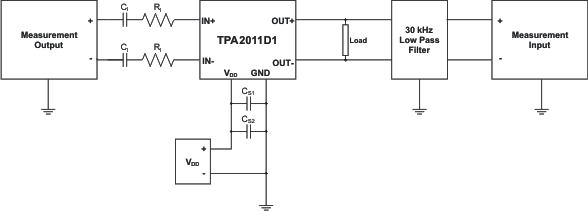
TPA2011D1 tst_stup_los626.gif
1. Input resistor RI = 150kΩ gives a gain of 6 dB which is used for all the graphs
2. CI was shorted for any common-mode input voltage measurement. All other measurements were taken with CI = 0.1-μF (unless otherwise noted).
3. CS1 = 0.1μF is placed very close to the device. The optional CS2 = 10μF is used for datasheet graphs.
4. The 30-kHz low-pass filter is required even if the analyzer has an internal low-pass filter. An RC low-pass filter (1kΩ, 4700pF) is used on each output for the data sheet graphs.
Figure 28. Test Setup for Typical Application Graphs