SLPS624A December   2016  – March 2019 CSD18512Q5B

PRODUCTION DATA.  
  1. 1Features
  2. 2Applications
  3. 3Description
    1.     Top View
      1.      Device Images
        1.       RDS(on) vs VGS
        2.       Gate Charge
  4. 4Revision History
  5. 5Specifications
    1. 5.1 Electrical Characteristics
    2. 5.2 Thermal Information
    3. 5.3 Typical MOSFET Characteristics
  6. 6Device and Documentation Support
    1. 6.1 Community Resources
    2. 6.2 Trademarks
    3. 6.3 Electrostatic Discharge Caution
    4. 6.4 Glossary
  7. 7Mechanical, Packaging, and Orderable Information
    1. 7.1 Q5B Package Dimensions
    2. 7.2 Recommended PCB Pattern
    3. 7.3 Recommended Stencil Pattern
    4. 7.4 Q5B Tape and Reel Information

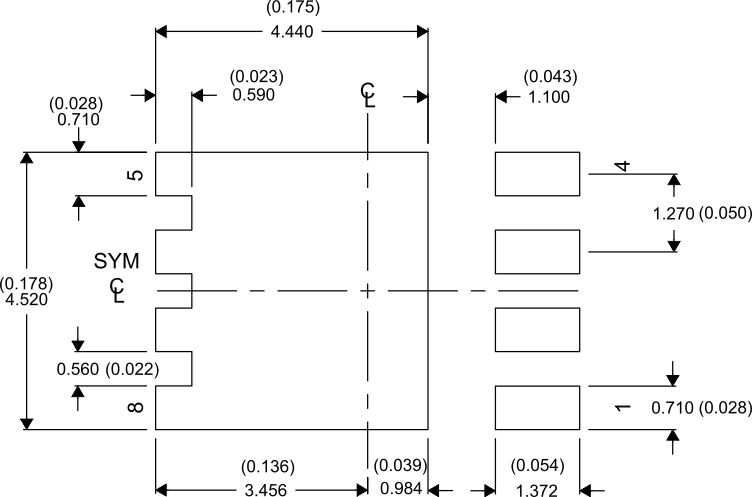
Recommended PCB Pattern

CSD18512Q5B Recommended_PCB.gif

For recommended circuit layout for PCB designs, see application note SLPA005Reducing Ringing Through PCB Layout Techniques.