SLUAA33A April 2020 – October 2022 BQ25970
3.3 PCB Layout Tips for BQ25970
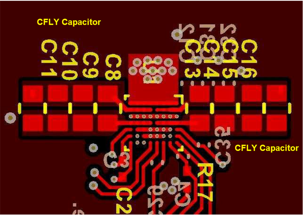
Proper PCB layout ensures good performance, so the designer must pay attention on PCB layout as the PCB layout sample in Figure 3-5 shows.
 Figure 3-5 BQ25970 PCB Layout
- CFLY capacitors are placed close to the BQ25970 device, the power trace should be short and wide to decrease power loss on the PCB trace.
- Connect the GND pin to the main ground plane directly to get better thermal sink and better EMI performance.
- The width of the external MOSFET gate driving trace between the OVPGATE pin and the external MOSFET gate should be 10 mil or more because of high di/dt when OVPGATE is active. Also, it is better to surround this driving trace with a ground wire to avoid any noise interference.
- The battery sense trace BATP and BATN should be routed as differential traces, and connect them to the battery socket terminal directly. If possible, surround them with ground trace to avoid noise interference.