SLUAAE9B May 2022 – November 2023 TPS62860 , TPS62861 , TPS62864 , TPS62866 , TPS62868 , TPS62869 , TPS62870 , TPS62870-Q1 , TPS62871 , TPS62871-Q1 , TPS62872 , TPS62872-Q1 , TPS62873 , TPS62873-Q1 , TPS62874-Q1 , TPS62875-Q1 , TPS62876-Q1 , TPS62877-Q1 , TPS6287B10 , TPS6287B25 , TPSM8287A06 , TPSM8287A12 , TPSM8287A15
- 1
- Abstract
- Trademarks
- 1 Introduction
- 2 Smart Routing and Tiny IC Packages
- 3 Selectable Forced-PWM/PSM operation
- 4 Dynamic Output Voltage Adjustment During Operation
- 5 Thermal Considerations
- 6 Droop Compensation
- 7 Step-Down Converter with an I2C Interface Selection Table
- 8 Conclusion
- 9 References
- 10Revision History
2 Smart Routing and Tiny IC Packages
A proper pinout assignment is critical to make sure a simple component placement and a small design size. It is also important to provide an easy access to all available pins on the package of the device. To integrate an I2C communication interface, two additional logic pins, SDA and SCL, need to be added. To allow easy routing without expensive microvias, the I2C pins should be added on the outside of the device.
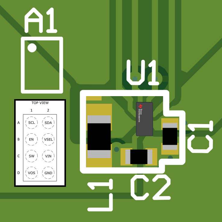
The TPS62861 combines a flexible design and a small design size. The TPS62861 is housed in a 8-pin tiny 0.7x1.4mm wafer chip scale package (WCSP). Figure 3-2 shows the PCB layout of the TPS62861 which is optimized for the design size of 12 mm² and has all pins accessible from the outside of the package. No vias are required for connecting to the IC.
 Figure 2-1 TPS62861 Layout Connecting all Pins Without Vias
Layout Matters: Solving Pinout Assignment Issues for DC/DC Converters in WCSP Packages is a technical article describing how a good pinout assignment can help for a small and simple implementation of a DC/DC converter with an I2C communication interface.