SLUAAG6 June 2022 BQ25180
1 Introduction
The BQ2518x are a 1-cell 1A linear battery chargers integrated circuit (IC) focusing on small solution size and ultra low quiescent current for optimal battery life. The BQ25180 and BQ25181 are the I2C controlled versions of the BQ2518x family of linear chargers. This board design demonstrates the smallest functional solution size for both the BQ25180 and BQ25181.
|
Figure 1-1 BQ25180 (WCSP) Pinout |
Figure 1-2 BQ25181 (QFN) Pinout |
The BQ25180 is an 8-pin WCSP (1.6 ✕ 1.1 mm) and the total solution size area is 7 mm2, including all the key components needed for operation. On the other hand, the BQ25181 is a 10-pin QFN (2 ✕ 2.2 mm) and the total solution size area is 12 mm2.
The BQ25180 in the WCSP package with the smallest solution size is ideal for wearables applications where the overall footprint is a critical design consideration. The BQ25181 in the QFN package with thermal-pad provides the best thermal performance in a small solution size for those applications which needs to operate at the high-end of power dissipation or need the additional two pins for extra configurability.
The small form factor area on this design incorporates the battery chargers and the bypass capacitors for IN, SYS and BAT pins, which are the key components needed for the charger to operate. In addition, the printed circuit board (PCB) includes the pads for the SDA and SCL pull up resistors, these however are not included on the solution size as they are typically shared on the I2C bus alongside the rest of the system.
The TS/MR pin on the BQ2518x devices, act as a dual function input which monitor the battery pack temperature and function as a manual reset pin to the part. On this board design the TS/MR pin includes a push button for resetting the device in parallel with a 10-kΩ resistor which simulates an attached battery pack at 25°C working under normal operation. On the BQ25181 board, also included are the external resistors pads for the charge enable (/CE) and the power good/general purpose output (PG/GPO) pins, which are the additional pins included on the QFN device.
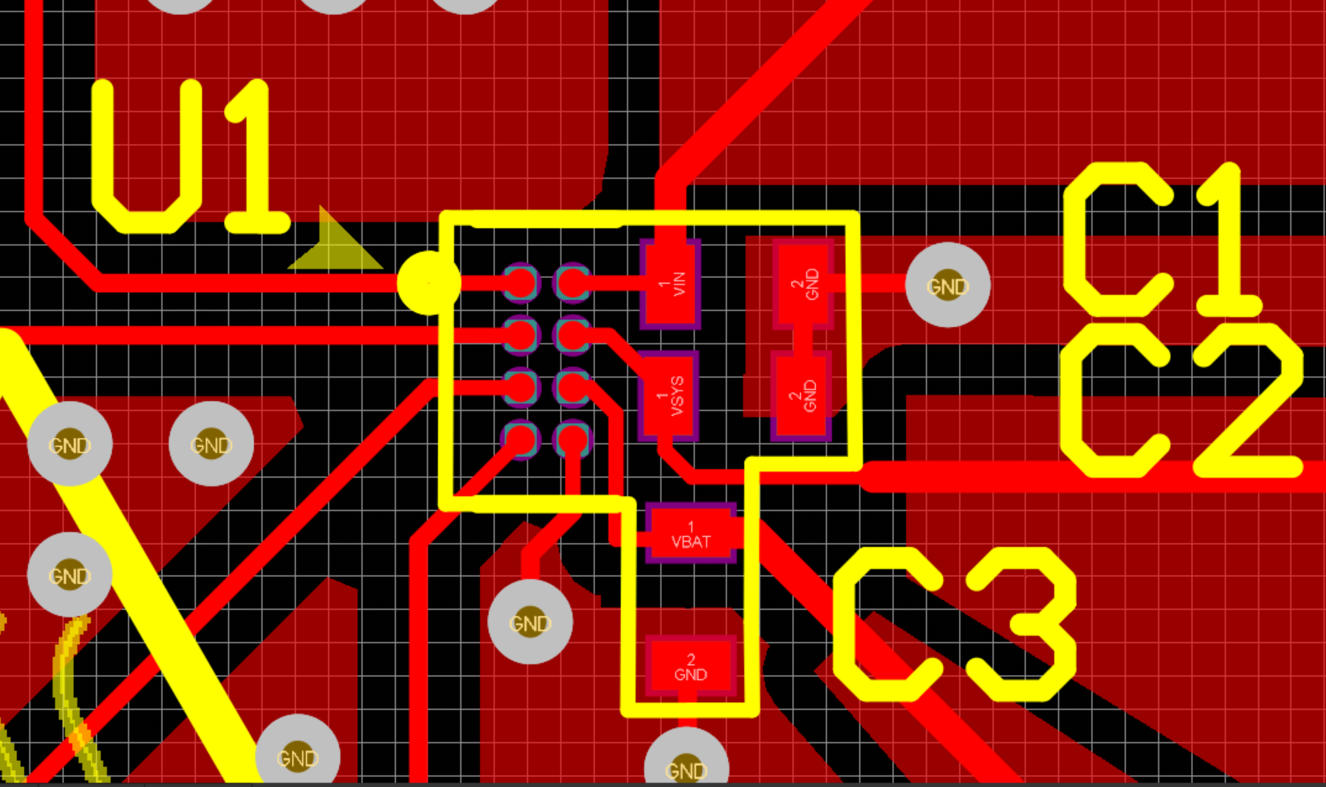
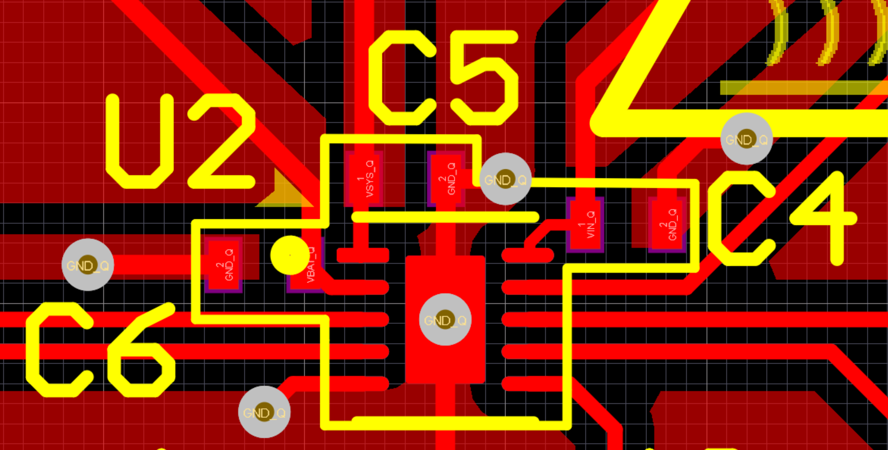
The boards are standard 62 mil 2-layer PCB with 1-oz copper, including mostly 6-mil traces with a 6-mil clearance and 26 mil diameter vias with a hole size of 10 mil. The 2-layer board design allows for an easy and cost-effective fanout routing without the need to use high density interconnect layout techniques. Figure 1-3 shows the BQ25180 fanout, which includes 5 mil traces extending to 6 mil away from the pads and vias. Figure 1-4 shows the BQ25181 fanout, which include 8-mil traces with one via with a hole size of 10 mil on the power-pad to aid with power dissipation. The total board size is 38 mm ✕ 38 mm for both the BQ25180 and BQ25181.

Figure 1-3 BQ25180 Fanout, 5-mils to 6-mils on Pads

Figure 1-4 BQ25181 Fanout, 8-mils on Pads