SLUAAN9 February 2023 BQ769142 , BQ76942 , BQ76952 , BQ76972 , ISO1640 , LM5168
2.2 Control Signals
As for the other relatively slow switching signals, like ALERT, TS2, RST_SHUT, DFETOFF, CFETOFF, use discrete level shifters or optocouplers which are more cost-effective.
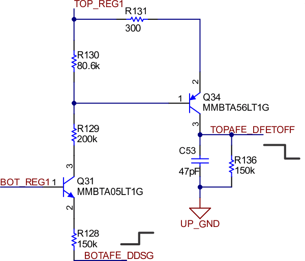
Since the bottom BQ769x2 monitors the pack current, bottom group cell voltages and temperature, but also the charge and discharge MOSFET are driven by the top BQ769x2, allow the bottom BQ769x2 to turn off the charge and discharge MOSFETs directly without the host MCU. This is especially helpful for faster protections like SCD. In TIDA-010247, the DDSG and DCHG pins of the bottom BQ769x2 are configured for DDSG and DCHG functionality and the DFETOFF and CFETOFF pins of the top BQ769x2 are configured for DFETOFF and CFETOFF functionality. Two discrete level shifters allow the bottom BQ769x2 DDSG and DCHG to control the top BQ769x2 DFETOFF and CFETOFF separately. The bottom BQ769x2 DDSG is also ORed with an MCU IO to drive Q47 to make sure the discharge MOSFET is completely off, so DDSG has to be configured as active-high (more details for the MOSFET driver are described in High side N-Channel MOSFET). But DCHG is configured as active-low to save power.

Figure 2-2 DDSG Level-Shifter Circuit