SLUS670C JULY 2005 – January 2015 TPS51120
PRODUCTION DATA.
- 1 Features
- 2 Applications
- 3 Description
- 4 Revision History
- 5 Pin Configuration and Functions
- 6 Specifications
-
7 Detailed Description
- 7.1 Overview
- 7.2 Functional Block Diagram
- 7.3
Feature Description
- 7.3.1 PWM Operation
- 7.3.2 Adaptive On-Time Control
- 7.3.3 Light Load Operation
- 7.3.4 Forced PWM Operation
- 7.3.5 5-V, 100-mA, LDO and Switchover (VREG5)
- 7.3.6 3.3-V, 100-mA, LDO and Switchover (VREG3)
- 7.3.7 2-V, 50-uA Sink - Source Reference (VREF2)
- 7.3.8 Low-Side Driver
- 7.3.9 High-Side Driver
- 7.3.10 Soft-Start
- 7.3.11 Soft-Stop
- 7.3.12 Powergood
- 7.3.13 Current Sensing and Overcurrent Protection
- 7.3.14 Overvoltage Protection
- 7.3.15 Undervoltage Protection
- 7.3.16 5-V Supply and UVLO Protection
- 7.3.17 VIN Line Sag Protection (Dynamic UVP)
- 7.3.18 Thermal Shutdown
- 7.4 Device Functional Modes
- 7.5 Programming
- 8 Application and Implementation
- 9 Power Supply Recommendations
- 10Layout
- 11Device and Documentation Support
- 12Mechanical, Packaging, and Orderable Information
7 Detailed Description
7.1 Overview
The TPS51120 is a highly sophisticated dual synchronous buck controller targeted for notebook I/O and system bus supply solutions. It support both D-CAP mode and current mode. With D-CAP control mode implemented, compensation network can be removed. Besides, the fast transient response also reduced the output capacitance. In case very low output ripple voltage needed, current mode can be implemented with simplified loop compensation and ceramic output capacitors.
7.2 Functional Block Diagram
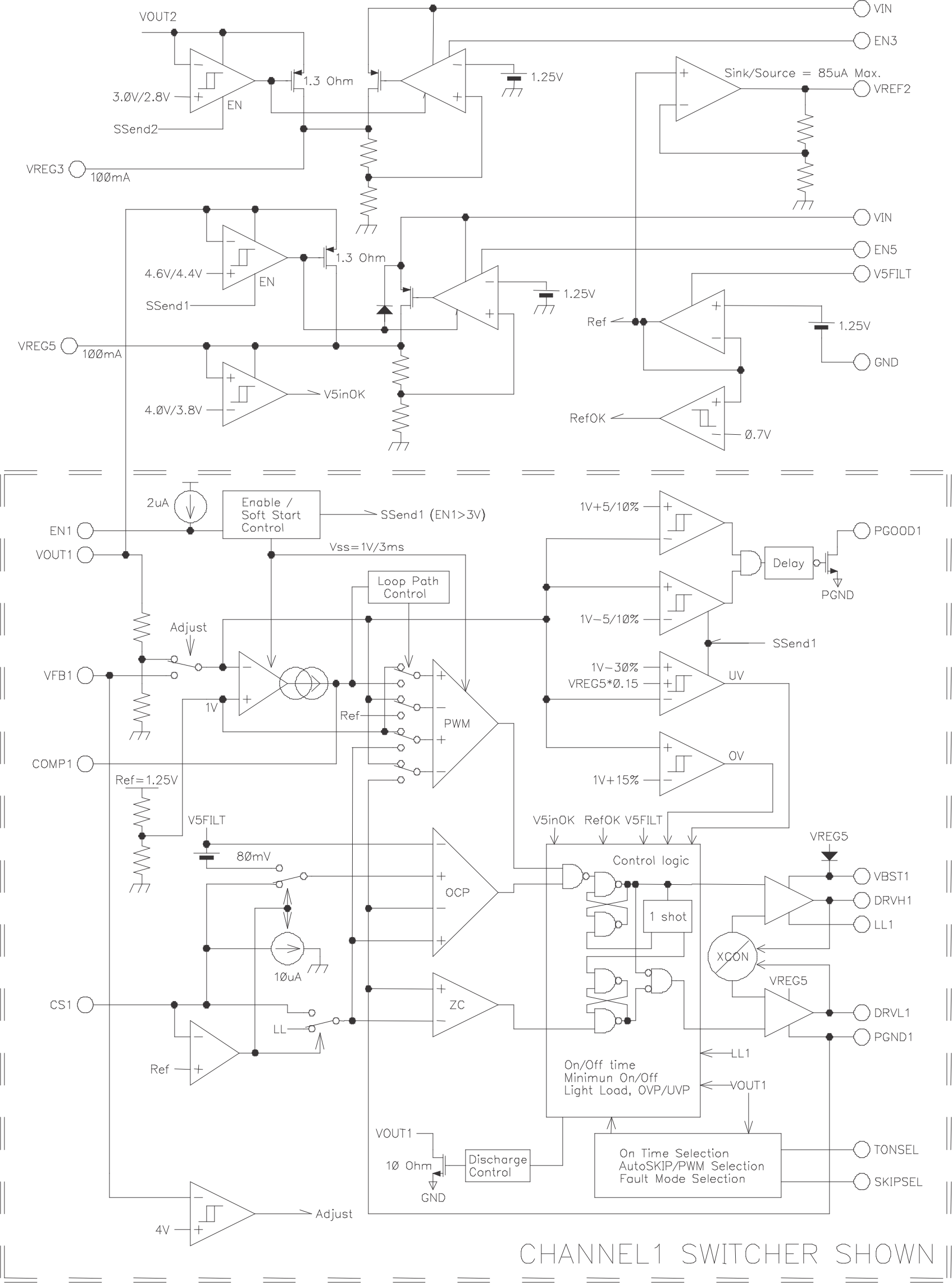 Figure 27. Block Diagram (One Channel Only Shown)
7.3 Feature Description
7.3.1 PWM Operation
The switching mode power supply (SMPS) block of TPS51120 supports an adaptive on time control pulse-width-modulation (PWM). Switching frequency is selectable from four choices. The TPS51120 supports both true current mode control and D-CAP mode control, selectable up to the requirements from system design. All N-channel MOSFET totem-pole architecture is employed for external switches. The synchronous top (high-side) MOSFET is turned on, or is “SET”, at the beginning of each cycle. This MOSFET is turned off, or is “RESET” after a constant “on-time” period which is defined by the frequency of customer’s choice and input and output voltage ratio. For different control mode, the condition for the top MOSFET turn on again is different.
If current mode is implemented, then the top MOSFET is turned on again if inductor current is reduced to meet both conditions of:
- the current level corresponds to the error amount of output voltage and,
- below the overcurrent limit level
If D-CAP mode is implemented, then the top MOSFET is turned on again when both of below conditions is met:
- the internal or external feedback voltage cross with the internal 1-V reference and,
- the inductor current below the overcurrent limit level
Repeating operation in this manner, the controller regulates the output voltage. The synchronous bottom (lowside) or the rectifying MOSFET is turned on each cycle in the negative phase to the top MOSFET to keep the conduction loss minimum. The rectifying MOSFET turns off on the event reverse inductor current flow is detected. This enables seamless transition to skip mode function so that high efficiency is kept over a broad range of load current. At the beginning of the soft start period, the rectifying MOSFET remains in the off state until the top MOSFET is turned on for at least once.
7.3.2 Adaptive On-Time Control
The TPS51120 employs adaptive on time control scheme and does not have a dedicated oscillator on board. However, it works almost constant frequency over the entire input voltage range (pseudo-constant frequency) by feed-forwarding the input and output voltage into the on-time one-shot timer. The on-time is controlled inverse proportional to the input voltage and proportional to the output voltage so that the duty ratio is kept as VOUT/VIN technically with the same cycle time. The input voltage monitoring is accomplished through sensing the LL node, not at VIN node, during the ‘ON’ state. This eliminates the influence of the voltage drop across the top MOSFET to the frequency especially in heavy load condition. The VIN pin is not used for the on-time control but used only for the 5 V and 3.3 V regulators’ supply. The switching frequency is selectable from four combinations shown in the table below by setting TONSEL pin voltage. This allows the system design to pursue highest efficiency (5 V/180 kHz, 3.3 V/270 kHz), smallest components size (5 V/380 kHz, 3.3 V/580 kHz) or a good balance of both in the medium. Also shown in the table are the typical on-time for each frequency and 5 V, 3.3 V outputs at VIN=12. Output voltage feed-forward is enabled after the output voltage exceeds 1.0 V in order to achieve stable start up.
Table 1. Frequency Selection and Typical On-Time
| TONSEL CONNECTION | CH1(LL1=VIN=12 V) | CH2 (LL2=VIN=12 V) | ||
|---|---|---|---|---|
| FREQUENCY (kHz) | ON-TIME @ 5 V (ns) | FREQUENCY (kHz) | ON-TIME @ 3.3 V (ns) | |
| V5FILT | 180 | 2340 | 270 | 1030 |
| FLOAT (OPEN) | 220 | 1950 | 330 | 850 |
| VREF2 | 280 | 1490 | 430 | 650 |
| GND | 380 | 1111 | 580 | 480 |
7.3.3 Light Load Operation
TPS51120 automatically reduces switching frequency at light load condition to maintain high efficiency. This reduction of frequency is achieved smoothly and without an increase in load regulation. Detail operation is described as follows. As the output current decreases from heavy load condition, the inductor current is also reduced and eventually comes to the point that its ‘valley’ touches zero current, which is the boundary between continuous conduction and discontinuous conduction modes. The rectifying MOSFET is turned off when this zero inductor current is detected. The on-time is kept the same as that in the heavy load condition. As the load current further decreases, the converter runs in discontinuous conduction mode and it takes longer and longer to discharge the output capacitor to the level that requires next ‘ON’ cycle. This results in reducing the switching frequency. In reverse, when the output current increases from light load to heavy load, switching frequency increases to the constant predetermined frequency as the inductor current reaches to the continuous conduction. The transition load point to the light load operation IOUT(LL) (i.e. the threshold between continuous and discontinuous conduction mode) can be calculated as shown in Equation 1.

where f is the PWM switching frequency which is determined by TONSEL pin. Switching frequency versus output current in the light load condition is a function of L, f, VIN and VOUT, but it decreases almost proportional to the output current from the IOUT(LL) given in Equation 1.
7.3.4 Forced PWM Operation
Tying SKIPSEL to V5FILT or leaving it float force the part to operate in continuous conduction mode for entire load range by disabling zero inductor current detection. Switching frequency is kept at the frequency selected by TONSEL input. System designers may want to use this mode to avoid certain frequency in light load condition with the cost of low efficiency. However, please be aware the output has a capability to both sink and source current in this mode. If the output terminal is connected to a voltage source higher than the regulated voltage, the converter sinks current from the output and boosts the charge into the input capacitor. This may cause unexpected high voltage at VIN and may damage the part.
7.3.5 5-V, 100-mA, LDO and Switchover (VREG5)
A 5-V, 100-mA linear regulator is integrated in the TPS51120. This low drop-out (LDO) regulator services the main analog supply rail for the IC and provides the current for the gate drivers. The regulator is a PMOS type with transconductance control and the pole is determined by the value of output capacitance. Typically, the value of this capacitor must be greater than 4.7 μF. A 10-μF ceramic capacitor is recommended for a typical design. Current limit and thermal protection are included in the regulator. Additionally, if the VO1 voltage exceeds 4.8 V, then the regulator is switched off and the 5V rails are bootstrapped to the 5-V switcher output, improving the efficiency of the converter. A glitch-free switchover is accomplished. The VREG5 output voltage does not show a short “glitch” down to 4.8 V when this bootstrapping action is taken. The switchover impedance from VO1 to VREG5 is typically 1.3 Ω. Standby current is designed for 30-μA operation allowing the user to leave the regulator alive while maintaining maximum battery life. The EN5 pin is a high voltage input and can be tied to VBAT or left open to enable the 5-V regulator. This 5-V regulator must be enabled prior to enable switching regulators. Pull EN5 to ground to shut off the regulator. Disabling the regulator does not promise shutting down the switchers once 5 volts is supplied via the bootstrap path. Because switchover occurs, the 5-V switcher MUST be turned off with the LDO in order to shut down the device. EN5 does NOT function as a master disable.
7.3.6 3.3-V, 100-mA, LDO and Switchover (VREG3)
A 3.3-V, 100-mA linear regulator is integrated as a second regulator in the TPS51120. This LDO provides a handy standby supply for 3.3 V ‘Always On’ voltages in the notebook system. The characteristics of this LDO are identical to the 5V LDO except for the switchover voltage. Apply 10-μF ceramic capacitor from VREG3 to PGND in adjacent to the device. If the VO2 voltage exceeds 3.1 V, then this regulator is switched off and the 3.3 V rail is bootstrapped to the 3.3 V switcher. Note if the VO2 voltage is set higher by external feedback dividers, for example 5 V, that high voltage is presented at VREG3 after switchover. The EN3 pin is a low voltage input that can be tied to V5FILT or left open to enable the 3.3-V regulator. This 3.3-V regulator can be turned on or kept alive independent to the 5-V regulator.
7.3.7 2-V, 50-uA Sink - Source Reference (VREF2)
This is a handy reference for generating auxiliary voltages. The tolerance is ±2% over 50-μA load and 0°C to 85°C ambient temperature ranges. The four-state logic (SKIPSEL, TONSEL) takes advantage of this reference for additional selection modes. This reference is enabled when both EN3 and EN5 become high, shuts down after both switchers are turned off and VREG5 or VREG3 is shut down. Please refer to Table 3. If this output is forcibly tied down to ground, both SMPS are turned off without latch. Bypass VREF2 pin to GND by a 1-nF capacitor.
7.3.8 Low-Side Driver
The low-side gate driver, DRVL, is designed to drive high current low RDS(on) N-channel MOSFET(s). The maximum drive voltage is 5.5 V which is delivered from VREF5 pin. The instantaneous drive current is supplied from the output capacitor at the VREF5 pin. The average drive current is equal to the FET’s gate charge at VGS=5 V times switching frequency. The VREG5 pin voltage may contain high frequency noise due to parasitic inductance by wiring and pointing current flow into the gate capacitor. The drive capability is represented by its internal resistance, which are 3.5 Ω for VREG5 to DRVL and 1.5 Ω for DRVL to PGND. Adaptive dead time control generates delay times between top MOSFET off to bottom MOSFET on, and bottom MOSFET off to top MOSFET on, preventing the totem-pole switches to shoot through. Top MOSFET off is detected as LL-node voltage declining below 2 V. Bottom MOSFET off is detected as DRVL voltage become 1.1 V.
7.3.9 High-Side Driver
The high-side gate driver, DRVH, is designed to drive high current, low RDS(on) N-channel MOSFET(s). When configured as a LL-node referenced floating driver, connect 0.1-μF ceramic capacitor between corresponding VBST pin and LL pin. A 5-V bias voltage is delivered from VREG5 supply. VBST is internally connected to VREG5 through a high voltage PN diode. This internal diode provides sufficient gate voltage for ordinary 4.5-V drive power MOSFETs and helps reducing external component. However, in the case where the gate bias voltage is critical for driving the top MOSFET, application designer may add an external schottky diode from VREG5 pin to VBST pin. Note schottky diodes have quite high reverse leakage current at high temperature. The instantaneous drive current is supplied by the flying capacitor connected between VBST and LL pins. The average drive current is equal to the gate charge at VGS=5 V times switching frequency. The drive capability is represented by its internal resistance, which are 3.5-Ω for VBST to DRVH and 1.5Ω for DRVH to LL. The maximum recommended voltage that can be applied between DRVH pin and LL pin is 5.5 V, DRVH pin to PGND pin is 34 V.
7.3.10 Soft-Start
The TPS51120 has an internal 3-ms voltage-servo soft start for each channel. When the EN1 or EN2 pin exceeds 0.9 V, an internal DAC begins ramping up the reference voltage. Smooth control of the output voltage during start up is maintained. However, if a slower soft-start is required, an external capacitor may be tied from the EN1 or EN2 pin to GND. In this case, the TPS51120 charges the external capacitor with the integrated 2-μA current source. The lower of either the EN voltage slew rate or the internal soft start slew rate dominates the start-up ramp. In addition, if tracking discharge is required, the EN pin can be used to control the output voltage discharge smoothly. An approximate value for the soft start reference voltage as a function of EN voltage is VSSREF = (VENX – 0.9)/1.5 < 1 V. At the beginning of soft-start period, the rectifying MOSFET maintains an off state until the top MOSFET is turned on for at least once. This prevents high negative current to flow back from the output capacitor in the event of output capacitor pre-charged condition.
7.3.11 Soft-Stop
Discharge mode or ‘Soft Stop’ is always on during Faults or Disable. In this mode, an event that would cause the switcher to be turned off (EN1 or EN2 low, OVP, UVP, UVLO) causes the output to be discharged through 10-Ω transistor inside the VO terminal. The external rectifying MOSFET is not turned on for the soft off operation to avoid a chance to cause negative voltage at the output. Soft-stop time constant is a function of the output capacitance and the resistance of the discharge transistor. This discharge ensures that, upon restart, the regulated voltage always starts from zero volts. In case a SMPS is restarted before discharge completion, soft-stop is terminated and the switching resumes after the reference level comes back to the remaining output voltage.
7.3.12 Powergood
The TPS51120 has dedicated powergood output for each SMPS, PGOOD1 and PGOOD2. The PGOOD monitors are open drain 5-mA pull down outputs. These outputs are low on startup and stay low until the switcher feedback voltages are within a specified range for 256 clocks or approximately 1 ms. If the VFB pin falls outside the 10% tolerance band, the respective PGOOD pin goes low within microseconds. Then if the VFB pin comes back within 5% of target (1 V) for greater than 1 ms, then the respective PGOOD pin goes high again. The PGOOD pin should be typically pulled up through a 100 kΩ or greater value resistor to the V5FILT pin. Both PGOOD pins go low during fault conditions (Thermal Shutdown, UVLO, UVP, OVP) and Disable.
7.3.13 Current Sensing and Overcurrent Protection
The SMPS has cycle-by-cycle over current limiting. The inductor current is monitored during the rectifying MOSFET is on and the controller does not allow the next ON cycle while the current level is above the trip threshold. In order to provide good accuracy and cost effective solution, TPS51120 supports both of external resistor sensing and MOSFET RDS(on) sensing which are selected by CS terminal connection. For resistor sensing scheme, an appropriate current sensing resistor should be connected between the source terminal of the bottom MOSFET and PGND. CS pin is connected to the bottom MOSFET source terminal node. The inductor current is monitored by the voltage between PGND pin and CS pin. In this scheme, the trip level is fixed value of 80 mV. For RDS(on) sensing scheme, CS terminal is connected to V5FILT through a trip voltage setting resistor RTRIP. In this scheme, CS terminal sinks 10-μA ITRIP current and the trip level is set to the voltage across the RTRIP. The trip level should be in the range of 30 mV to 150 mV. This allows designer to select a variety of MOSFETs for the bottom arm. The inductor current is monitored by the voltage between PGND pin and LL pin so that LL pin should be connected to the drain terminal of the bottom MOSFET. ITRIP has 4500ppm/°C temperature slope, with respect to its 25°C value, to compensate the temperature dependency of the RDS(on). In either scheme, PGND is used as the positive current sensing node so that PGND pin should be connected to the proper current sensing device, i.e. the sense resistor or the source terminal of the bottom MOSFET. In an overcurrent condition, since the current to the output capacitor is limited while the load drags more, the output voltage tends to go down. It ends up with passing into the undervoltage protection and latches off as both DRVH and DRVL are at low level.
Table 2. Current Sensing Connection
| CS | Threshold | Temperature Coefficient (ppm/°C) |
|
|---|---|---|---|
| RDS(on) sensing | V5FILT | ITRIP × RTRIP / RDS(on) | 4500 |
| RSENSE sensing | Bottom FET source node (=RSENSE (-) node) | 80 mV / RSENSE | none |
7.3.14 Overvoltage Protection
For over voltage protection (OVP), the TPS51120 monitors VFB voltage. When the VFB voltage is higher than 115% of the target, the OVP comparator output goes high and the circuit latches both switchers. The offending channel is latched DRVH low and DRVL high, the other channel is simply latched as DRVH and DRVL at low. Be aware negative voltage may appear at the output terminal of the offending channel because of LC resonant configured by the power inductor and the output capacitor. The system designer is responsible to this negative voltage if any protection is need. The OVP propagation delay is less than 3 μs.
7.3.15 Undervoltage Protection
For under voltage protection (UVP), the TPS51120 monitors VFB voltage. When the VFB voltage is lower than 70% of the target and the UVP comparator output goes high, the internal UVP delay counter begins count. After the 128 clocks, approximately 0.5 ms, TPS51120 latches off both channels as DRVH and DRVL at low. This function is enabled after the softstart reference has exceeded the internal 1-V reference operation to ensure startup. Please refer to Table 4.
7.3.16 5-V Supply and UVLO Protection
TPS51120 has two 5-V terminals. VREG5 is the output of 5-V linear regulator. This terminal also serves as input pin for the gate driver circuits. Internal switchover FET is connected between this pin and VO1. V5FILT is the VCC supply input for the control circuitry on the chip. Connect with R-C low pass filter from VREG5 to this V5FILT to eliminate spiky high frequency noise. State definition pins such as SKIPSEL, TONSEL, VFB (fixed output case) and COMP (for D-CAP mode) or CS resistors that need stable 5V should refer to V5FILT. The part has 5-V supply under voltage lock out protection (UVLO) to prevent unpredictable operation under insufficient power. The TPS51120 monitors VREG5 voltage. When the VREG5 voltage is lower than UVLO threshold, the SMPS’s are shut off. The output discharge or ‘soft stop’ feature is enabled for the channel one and channel two. However, because the discharge circuit derives its power from the 5-V line, power must be presented long enough to ensure that discharge is complete during shutdown. Also, during power up, the TPS51120 attempts to discharge the output capacitor until the UVLO (on) threshold is reached. A 5-V UVLO is non-latch protection and is automatically resumed up on 5-V recovery.
7.3.17 VIN Line Sag Protection (Dynamic UVP)
Since the TPS51120 serves primarily as system power (i.e. used for generating 3.3 V and 5 V) it is very important that the system not enter UVP if the VIN supply has dropped below 6V. UVP would be caused by the 5-V output dropping due to input line sag. When the VIN pin drops below the 5-V regulator voltage, the 5-V regulator ‘tracks’ VIN (LDO operation). The UVP threshold is adjusted downward when the VREG5 is below 4.8 V. This ensures that 5-V supply UVLO trips before the latching UVP condition occurs and the system power can recover normally when VIN recovers. This feature is very useful for transient VIN events such as adapter insertion
7.3.18 Thermal Shutdown
The TPS51120 employs thermal shutdown for the switchers at 145°C. This is a non-latch protection with hysteresis of 10°C. Both switching regulators and both internal regulators stop. VREG5 and VREG3 LDOs may not turn on if the part is preheated above the recovery temperature before starting up. Reduce the temperature to or below TA = 85°C to resume operation safely.
Table 3. Enable Logic States (Vout1=5 V, Vout2=3.3 V)
| EN5(1) | EN3 | EN1 | EN2 | VREG5 | VREG3 | VREF2(2) | SMPS1 | SMPS2 |
|---|---|---|---|---|---|---|---|---|
| Low | Low | High or Low | High or Low | Off | Off | Off | Off | Off |
| Low-to-High | Low | High or Low | High or Low | LDO 5 V | Off | Off | Off | Off |
| Low | Low-to-High | High or Low | High or Low | Off | LDO 3.3 V | Off | Off | Off |
| Low-to-High | Low-to-High | Low | Low | LDO 5 V | LDO 3.3 V | On | Off | Off |
| High | High | Low | Low-to-High | LDO 5 V | SW 3.3 V | On | Off | On |
| High | High | Low-to-High | Low | SW 5 V | LDO 3.3 V | On | On | Off |
| High | High | High | High | SW 5 V | SW 3.3 V | On | On | On |
| High-to-Low | High-to-Low | High | High | SW 5 V | SW 3.3 V | On | On | On |
| High | High | High-to-Low | High-to-Low | LDO 5 V | LDO 3.3 V | On | Off | Off |
| High-to-Low | High | High-to-Low | High | Off | LDO 3.3 V | Off | Off | Off |
| High | High-to-Low | High | High-to-Low | SW 5 V | Off | On | On | Off |
| High | High-to-Low | Low | High-to-Low | LDO 5 V | Off | Off | Off | Off |
| High-to-Low | High | Low | Low | Off | LDO 3.3 V | Off | Off | Off |
| High | High-to-Low | Low | Low | LDO 5 V | Off | Off | Off | Off |
Table 4. Protection States (Vout1 = 5 V, Vout2 = 3.3 V)
| DRVH1 | DRVL1 | DRVH2 | DRVL2 | PGOOD1 PGOOD2 |
VREG5 | VREG3 | VREF2 | FOR RESTART |
|
|---|---|---|---|---|---|---|---|---|---|
| UVPch1 | Low | Low | Low | Low | Low/Low | LDO 5 V | LDO 3.3 V | On | Toggle EN1 |
| UVPch2 | Low | Low | Low | Low | Low/Low | LDO 5 V | LDO 3.3 V | On | Toggle EN2 |
| OVPch1 | Low | High | Low | Low | Low/Low | LDO 5 V | LDO 3.3 V | On | Toggle EN1 |
| OVPch1 | Low | Low | Low | High | Low/Low | LDO 5 V | LDO 3.3 V | On | Toggle EN2 |
| Thermal SHDN | Low | Low | Low | Low | Low/Low | Off | Off | Off | Lower Package Temperature |
| VIN < 5.0 | Normal | Normal | Normal | Normal | Low/Normal | SW 5 V | SW 3.3 V | On | Raise VIN |
| VREG UVLO |
Low | Low | Low | Low | Low/Low | LDO but dropping | LDO 3.3 V | On | Raise VIN, Reduce 5V current |
| OCPch1 | Limited Duty | Estended Duty | Normal | Normal | Low/Normal | LDO 5 V | SW 3.3 V | On | Reduce CH1 Current |
| OCPch2 | Normal | Normal | Limited Duty | Estended Duty | Normal/Low | SW 5 V | LDO 3.3 V | On | Reduce CH2 Current |
| EN1 Low | Low | Low | Normal | Normal | Low/Normal | LDO 5 V | SW 3.3 V | On | Float or tie to VREG5 |
| EN2 Low | Normal | Normal | Low | Low | Normal/Low | SW 5 V | LDO 3.3 V | On | Float or tie to VREG5 |
| EN1, EN2, EN3 Low | Low | Low | Low | Low | Low/Low | LDO 5 V | Off | Off | Float EN3, then float EN1,2 or tie to VREG5 |
| EN5, EN1 Low | Low | Low | Low | Low | Low/Low | Off | LDO 3.3 V | Off | Float EN5 or tie to VBAT, tie EN1 to VREG5 |
7.4 Device Functional Modes
7.4.1 Current Mode
The current mode scheme is a sequence of feedback control described as follows. The output voltage is monitored at the middle point of voltage divider resistors and fed back to a transconductance amplifier. The amplifier outputs target current level proportional to error amount between the feedback voltage and the internal 1 V reference voltage. The inductor current level is monitored during the off-cycle, when rectifying MOSFET is turned on. The PWM comparator compares the inductor current signal with this target current level that is indicated at the COMP pin voltage. When both signals are equal (at the valley of the current sense signal), the comparator provides the “SET” signal to the gate driver latch. The current mode option has relatively higher flexibility by the external compensation network provided to the COMP pin. And it is suitable for lowest ripple design with output capacitor(s) having ultra-low ESR. When sensing the inductor current, accuracy and cost always trades off. In order to give the circuit designer a choice between these two, TPS51120 supports both of external resistor sensing and MOSFET RDS(on) sensing. Please contact factory for current mode EVM with RSENSE capability.
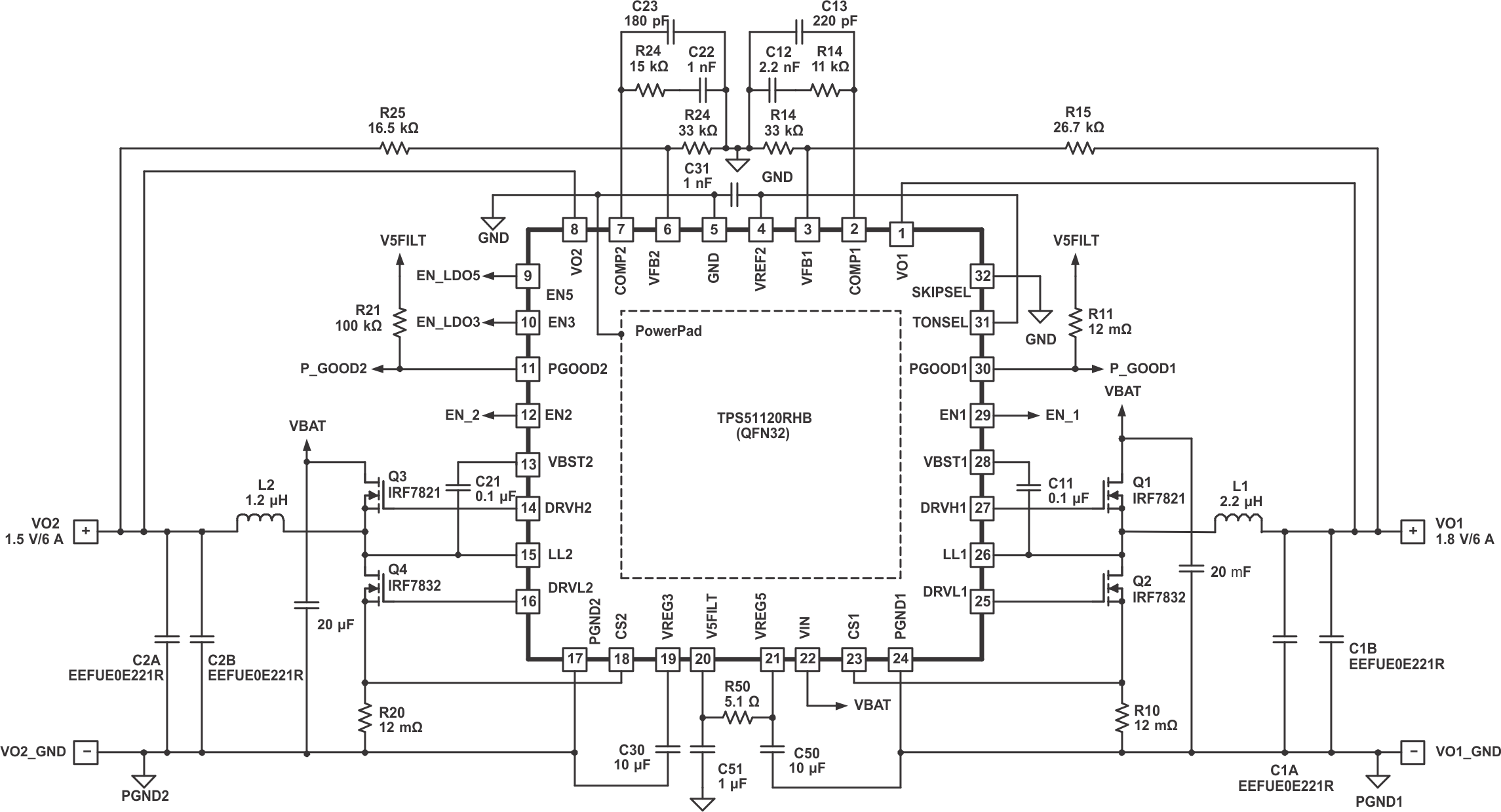 Figure 28. Current Mode, External 1.8-V / 6-A, 1.5-V / 6-A, RSENSE Sensing
7.4.1.1 Current Mode Operation
A buck converter using TPS51120 current mode operation can be partitioned into three portions, a voltage divider, an error amplifier and a switching modulator. By linearizing the s witching modulator, we can derive the transfer function of the whole system. Since current mode scheme directly controls the inductor current, the modulator can be linearized as shown in Figure 29.
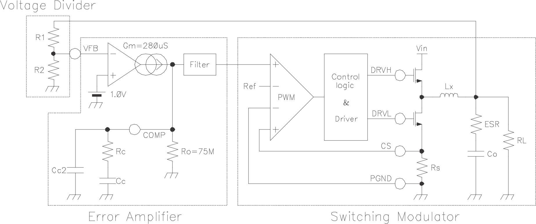 Figure 29. Linearizing the Modulator
Here, the inductor is located inside the local feedback loop and its inductance does not appear in the small signal model. As a result, a modulated current source including the power inductor can be modeled as a current source with its transconductance of 1/RS and the output capacitor represent the modulator portion. This simplified model is applicable in the frequency space up to approximately a half of the switching frequency. One note is, although the inductance has no influence to small signal model, it has influence to the large signal model as it limits slew rate of the current source. This means the buck converter’s load transient response, one of the large signal behaviors, can be improved by using smaller inductance without affecting the loop stability.
Total open loop transfer function of the whole system is given by Equation 2.

Assuming RL>>ESR, RO>>RC and CC>>CC2, each transfer function of three block is shown in Equation 3 through Equation 5.
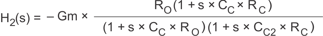
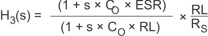
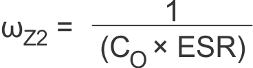
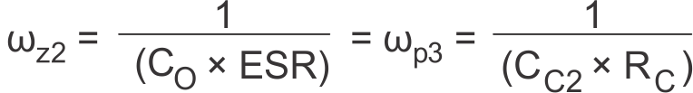
There are three poles and two zeros in H(s). Each pole and zero is given by Equation 6 through Equation 10.
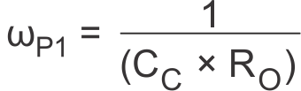
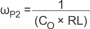
Usually, each frequency of those poles and zeros is lower than the 0 dB frequency, f0. However, the f0 should be kept under 1/3 of the switching frequency to avoid effect of switching circuit delay. The f0 is given by next equation Equation 11.

Based on small signal analysis above, the external components can be selected by following manner.
- Choose the inductor.The inductance value should be determined to give the ripple current of approximately 1/4 to 1/2 of maximum output current.
- Choose rectifying (bottom) MOSFET. When RDS(on) sensing scheme is selected, the rectifying MOSFET’s on-resistance is used as this RS so that lower RDS(on) does not always promise better performance. In order to clearly detect inductor current, minimum RS recommended is to give 15 mV or larger ripple voltage with the inductor ripple current. This promises smooth transition from CCM to DCM or vice versa. Upper side of the RDS(on) is of course restricted by the efficiency requirement, and usually this resistance affects efficiency more at high load conditions. When using external resistor current sensing, there is no restriction for low RDS(on). However, the current sensing resistance RS itself affects the efficiency.
- Choose output capacitor(s). If organic semiconductor capacitors (OS-CON) or specialty polymer capacitors (SP-CAP), are used, the ESR to achieve required ripple value at a stable state or transient load condition determines the amount of capacitor(s) need, and capacitance is then enough to satisfy stable operation. The peak-to-peak ripple value can be estimated by ESR times the inductor ripple current for stable state, or ESR times the load current step for a fast transient load response. In case of ceramic capacitor(s), usually ESR is small enough to meet ripple requirement. On the other hand, transient undershoot and overshoot driven by output capacitance becomes the key factor to determine the capacitor(s).
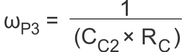
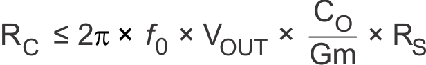
- Determine f0 and calculate RC using Equation 14. Note that higher RC shows faster transient response in cost of unstableness. If the transient response is not enough even with high RC value, try increasing the output capacitance. Recommended f0 is f/4.
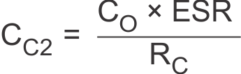
- Calculate CC2. The purpose of this capacitance is to cancel the zero caused by ESR of the output capacitor. If ceramic capacitor are used, there is no need for CC2.
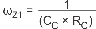
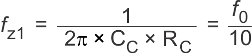
- Calculate CC. Purpose of CC is to cut DC component to obtain high DC feedback gain. However, as it causes phase delay, another zero to cancel this effect at f0 frequency is need. This zero, ωz1, is determined by CC and RC. Recommended ωz1 is 10 times lower to the f0 frequency.
- In case of adjustable mode, determine the value of R1 and R2. Recommended R2 value is from 10 kΩ to 20 kΩ. Determine R1 using Equation 18.

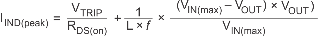
The inductor also needs to have low DCR to achieve good efficiency, as well as enough room above peak inductor current before saturation. The peak inductor current can be estimated in Equation 13.

7.4.2 D-Cap Mode
The D-CAP mode operation is enabled by tying the COMP pin to V5FILT. In this mode, the PWM comparator monitors the feedback voltage directly and compares the voltage with the internal 1-V reference. When both signals are equal at the valley of the voltage sense signal, the comparator provides the “SET” signal to the top MOSFET gate driver. Because the compensation network is implemented on the part and the output waveform itself is used as the error signal, external circuit design is largely simplified. Another advantage of the D-CAP mode is its inherent fast transient response. A trade-off is a sufficient amount of ESR required in the output capacitor. SPCAP or POSCAP is recommended. The inductor current information is still used in the D-CAP mode for over current protection and light load operation. Do NOT neglect current sensing design in this mode. To summarize, the D-CAP mode is suitable for the lowest external component count with the fastest transient response, but with relatively large ripple voltage. It is easy to design the loop once appropriate output capacitor and inductor current ripple is selected.
 Figure 30. D-Cap Mode, Fixed 5-V / 6-A, 3.3-V/6-A, RDS(on) Sensing
7.4.2.1 D-Cap Mode Operation
A buck converter system using D-CAP mode can be simplified as shown in Figure 31.
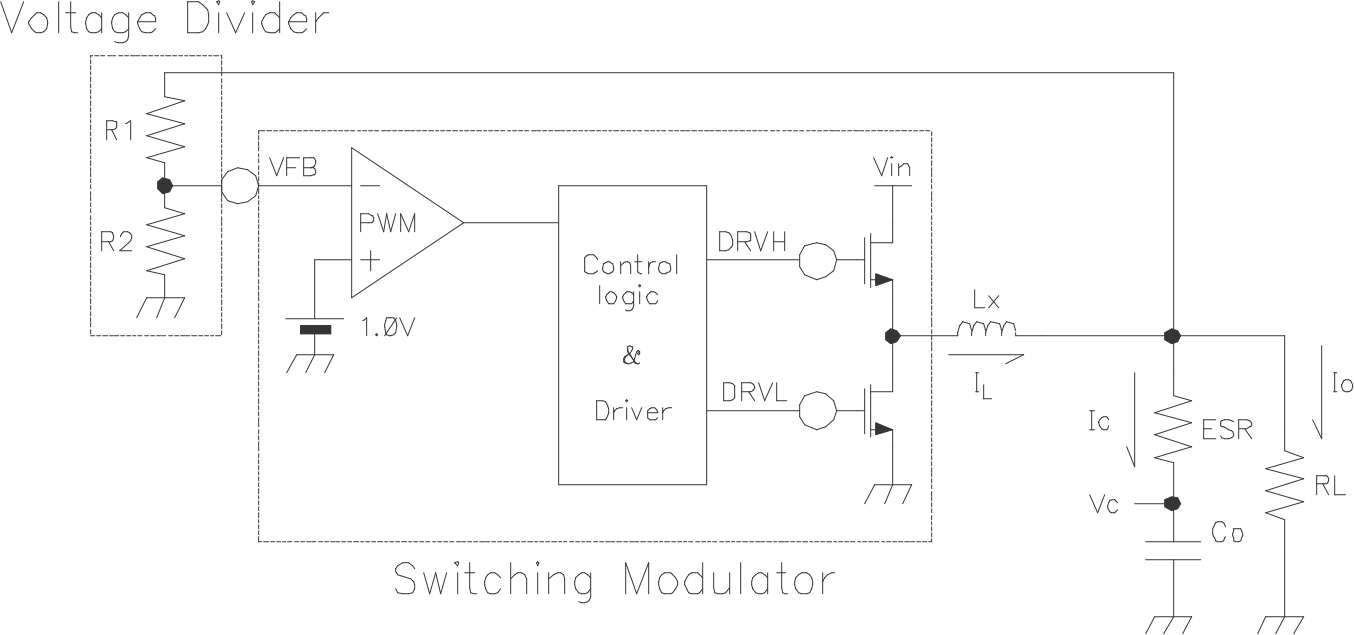 Figure 31. Linearizing the Modulator
The VO voltage is compare with internal reference voltage after divider resistors (Internal resistor mode. For adjustable mode, the comparison is directly at VFB). The PWM comparator determines the timing to turn on top MOSFET. The gain and speed of the comparator is high enough to keep the voltage at the beginning of each on cycle (or the end of off cycle) substantially constant. The DC output voltage may have line regulation due to ripple amplitude that slightly increases as the input voltage increase.
For the loop stability, the 0-dB frequency, f0, defined below need to be lower than 1/3 of the switching frequency.
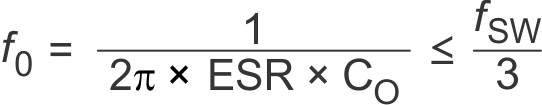
As f0 is determined solely by the output capacitor’s characteristics, loop stability of D-CAP mode is determined by the capacitor’s chemistry. For example, specialty polymer capacitors (SP-CAP) have Co in the order of several 100 μF and ESR in range of 10 mΩ. These produce an f0 in the order of 100 kHz or less and the loop is stable. However, ceramic capacitors have f0 at more than 700 kHz, which is not suitable for this operational mode.
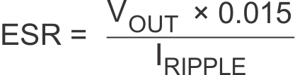
Although D-CAP mode provides many advantages such as ease-of-use, minimum external components configuration and extremely short response time, due to not employing an error amplifier in the loop, sufficient amount of feedback signal needs to be provided by external circuit to reduce jitter level. The required signal level is approximately 15 mV at comparing point, either the internal or external VFB voltages. The output capacitor’s ESR should meet this requirement.
The external components selection is much simple in D-CAP mode.
- Choose inductor based on frequency and acceptable ripple current.
- Choose output capacitor(s).Organic semiconductor capacitor(s) or specialty polymer capacitor(s) are recommended. Determine ESR to meet required ripple voltage above. A quick approximation is shown in Equation 20.
7.5 Programming
The TPS51120 has varieties of configurations choice. It is important to tailor appropriately with regard to the system design requirements. Table below shows programming table for the control scheme selection, frequency selection, output voltage selection and skip selection. Faults-off disables UVP, OVP and UVLO. This is mainly intended for debugging purpose. Enable states and possible connections for the LDO’s EN3, EN5 pins and SMPS’s EN1, EN2 pins are also shown.
Table 5. Function Programming Table
| PIN | GND | VREF2 | FLOAT | V5FILT |
|---|---|---|---|---|
| COMP | N/A | N/A | Current Mode (apply R-C network) |
D-CAP Mode |
| TONSEL (CH1/CH2) [kHz] | 380 / 580 | 280 / 430 | 220 / 330 | 180 / 270 |
| VFB1 | Adjustable output (connect to the resistor divider) | 5V fixed output | ||
| VFB2 | Adjustable output (connect to the resistor divider) | 3.3 V fixed output | ||
| SKIPSEL | AUTO-SKIP | AUTO-SKIP (FAULTS OFF) | PWM | PWM |
| EN1, EN2 | Switcher Off | Not used | Switcher on | Switcher on |
| EN3, EN5 | LDO Off | Not used | LDO on | LDO on (EN3 only) |