SLUS670C JULY 2005 – January 2015 TPS51120
PRODUCTION DATA.
- 1 Features
- 2 Applications
- 3 Description
- 4 Revision History
- 5 Pin Configuration and Functions
- 6 Specifications
-
7 Detailed Description
- 7.1 Overview
- 7.2 Functional Block Diagram
- 7.3
Feature Description
- 7.3.1 PWM Operation
- 7.3.2 Adaptive On-Time Control
- 7.3.3 Light Load Operation
- 7.3.4 Forced PWM Operation
- 7.3.5 5-V, 100-mA, LDO and Switchover (VREG5)
- 7.3.6 3.3-V, 100-mA, LDO and Switchover (VREG3)
- 7.3.7 2-V, 50-uA Sink - Source Reference (VREF2)
- 7.3.8 Low-Side Driver
- 7.3.9 High-Side Driver
- 7.3.10 Soft-Start
- 7.3.11 Soft-Stop
- 7.3.12 Powergood
- 7.3.13 Current Sensing and Overcurrent Protection
- 7.3.14 Overvoltage Protection
- 7.3.15 Undervoltage Protection
- 7.3.16 5-V Supply and UVLO Protection
- 7.3.17 VIN Line Sag Protection (Dynamic UVP)
- 7.3.18 Thermal Shutdown
- 7.4 Device Functional Modes
- 7.5 Programming
- 8 Application and Implementation
- 9 Power Supply Recommendations
- 10Layout
- 11Device and Documentation Support
- 12Mechanical, Packaging, and Orderable Information
10 Layout
10.1 Layout Guidelines
Certain points must be considered before starting a layout work using the TPS51120.
- Connect RC low-pass filter from VREG5 to V5FILT, 1 μF and 5.1 Ω are recommended. Place the filter capacitor close to the device, within 12 mm (0.5 inches) if possible.
- VREG5 and VREG3 require at least 4.7 μF, VREF2 requires a 1-nF ceramic bypass capacitor which should be placed close to the device and traces should be no longer than 10 mm.
- Connect the overcurrent setting resistors from CSx to V5FILT (NOT VREG5) and close to the device, right next to the device if possible. The trace from CSx to V5FILT should avoid coupling to high-voltage switching node.
- In the case of using adjustable output voltage with an external resistor divider, the discharge path (VOx) should have a dedicated trace to the output capacitor; separate from the output voltage sensing trace, and use 1.5 mm or wider trace with no loops. Make the feedback current setting resistor (the resistor between VFBx to GND) is tied close to the device’s GND. Place on the component side and avoid vias between this resistor and the device.
- Connections from the drivers to the respective gate of the high-side or the low-side MOSFET should be as short as possible to reduce stray inductance. Use 0.65 mm (25 mils) or wider trace.
- All sensitive analog traces and components such as VOx, COMPx, VFBx, VREF2, GND, ENx, PGOODx, CSx, V5FILT, TONSEL and SKIPSEL should be placed away from high-voltage switching nodes such as LLx, DRVLx or DRVHx nodes to avoid coupling. Use internal layer(s) as ground plane(s) and shield feedback trace from power traces and components.
- Gather ground terminal of VIN capacitor(s), VOUT capacitor(s) and source of low-side MOSFETs as close as possible. GND (signal ground) and PGNDx (power ground) should be connected strongly together near the device. PCB trace defined as LLx node, which connects to source of high-side MOSFET, drain of low-side MOSFET and high-voltage side of the inductor, should be as short and wide as possible.
- In order to effectively remove heat from the package, prepare thermal land and solder to the package’s thermal pad. Three by three or more vias with a 0.33-mm (13mils) diameter connected from the thermal land to the internal ground plane should be used to help dissipation. Do NOT connect PGNDx to this thermal land underneath the package.
10.2 Layout Example
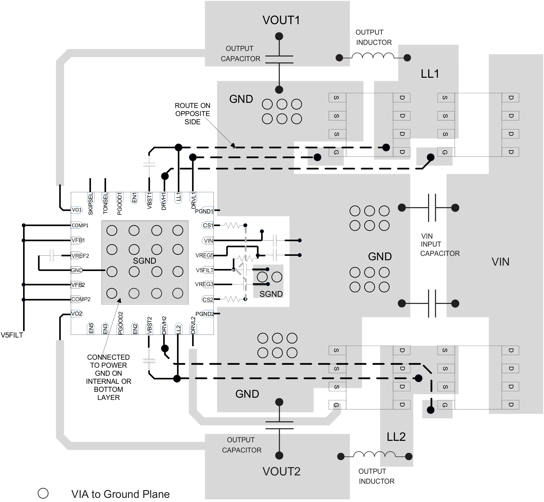 Figure 41. Layout Example