SLUSD37E October   2017  – November 2019 UCC28056

PRODUCTION DATA.  

  1. Features
  2. Applications
  3. Description
    1.     No Load Power
      1.      Device Images
        1.       Simplified Application
  4. Revision History
  5. Device Comparison Tables
  6. Pin Configuration and Functions
    1.     Pin Functions
  7. Specifications
    1. 7.1 Absolute Maximum Ratings
    2. 7.2 ESD Ratings
    3. 7.3 Recommended Operating Conditions
    4. 7.4 Thermal Information
    5. 7.5 Electrical Characteristics
    6. 7.6 Typical Characteristics
  8. Detailed Description
    1. 8.1 Overview
    2. 8.2 Functional Block Diagram
    3. 8.3 Feature Description
      1. 8.3.1 CrM/DCM Control Principle
      2. 8.3.2 Line Voltage Feed-Forward
        1. 8.3.2.1 Peak Line Voltage Detection
      3. 8.3.3 Valley Switching and CrM/DCM Hysteresis
        1. 8.3.3.1 Valley Delay Adjustment
      4. 8.3.4 Transconductance Amplifier with Transient Speed-up Function
      5. 8.3.5 Faults and Protections
        1. 8.3.5.1 Supply Undervoltage Lockout
        2. 8.3.5.2 Two Level Over-Current Protection
          1. 8.3.5.2.1 Cycle-by-Cycle Current Limit Ocp1
          2. 8.3.5.2.2 Ocp2 Gross Over-Current or CCM Protection
        3. 8.3.5.3 Output Over-Voltage Protection
          1. 8.3.5.3.1 First Level Output Over-Voltage Protection (Ovp1)
          2. 8.3.5.3.2 Second Level Over-Voltage Protection (Ovp2)
        4. 8.3.5.4 Thermal Shutdown Protection
        5. 8.3.5.5 Line Under-Voltage or Brown-In
      6. 8.3.6 High-Current Driver
    4. 8.4 Controller Functional Modes
      1. 8.4.1 Burst Mode Operation
      2. 8.4.2 Soft Start
  9. Application and Implementation
    1. 9.1 Application Information
    2. 9.2 Typical Application
      1. 9.2.1 Design Requirements
      2. 9.2.2 Detailed Design Procedure
        1. 9.2.2.1 Custom Design With WEBENCH® Tools
        2. 9.2.2.2 Power Stage Design
          1. 9.2.2.2.1 Boost Inductor Design
          2. 9.2.2.2.2 Boost Switch Selection
          3. 9.2.2.2.3 Boost Diode Selection
          4. 9.2.2.2.4 Output Capacitor Selection
        3. 9.2.2.3 ZCD/CS Pin
          1. 9.2.2.3.1 Voltage Spikes on the ZCD/CS pin Waveform
        4. 9.2.2.4 VOSNS Pin
        5. 9.2.2.5 Voltage Loop Compensation
          1. 9.2.2.5.1 Plant Model
          2. 9.2.2.5.2 Compensator Design
      3. 9.2.3 Application Curves
  10. 10Power Supply Recommendations
  11. 11Layout
    1. 11.1 Layout Guidelines
      1. 11.1.1 VOSNS Pin
      2. 11.1.2 ZCD/CS Pin
      3. 11.1.3 VCC Pin
      4. 11.1.4 GND Pin
      5. 11.1.5 DRV Pin
      6. 11.1.6 COMP Pin
    2. 11.2 Layout Example
  12. 12Device and Documentation Support
    1. 12.1 Custom Design With WEBENCH® Tools
    2. 12.2 Receiving Notification of Documentation Updates
    3. 12.3 Community Resources
    4. 12.4 Trademarks
    5. 12.5 Electrostatic Discharge Caution
    6. 12.6 Glossary
  13. 13Mechanical, Packaging, and Orderable Information

Peak Line Voltage Detection

UCC28056 internally reconstructs the input voltage waveform for the purpose of Peak Line voltage sensing and Zero Current Detection (ZCD). In DCM or CrM mode the cycle average voltage across the Boost inductor must be zero. UCC28056 generates an internal representation of input voltage by extracting the Drain waveform from the ZCD/CS pin waveform and filtering it to extract the average Drain voltage across a switching cycle (VInSyn(θ))

The digital peak detector selects the value of GFF based upon the highest comparator threshold crossed over the period THLinMax . The switch to a higher GFF value is implemented as soon as the corresponding threshold is crossed. The switch to a lower GFF value is only implemented once the period THLinMax expires and the peak detector has captured the Line voltage peak. The THLinMax timer is not synchronized to the Line operating frequency.

Prior to the start of switching operation, at power - up or after a Burst - OFF period, the ZCD/CS pin voltage is sampled and used to select the appropriate starting GFF level. This method assumes that the input rectifier and capacitor after the rectifier bridge have captured the peak Line voltage during the period of no switching.
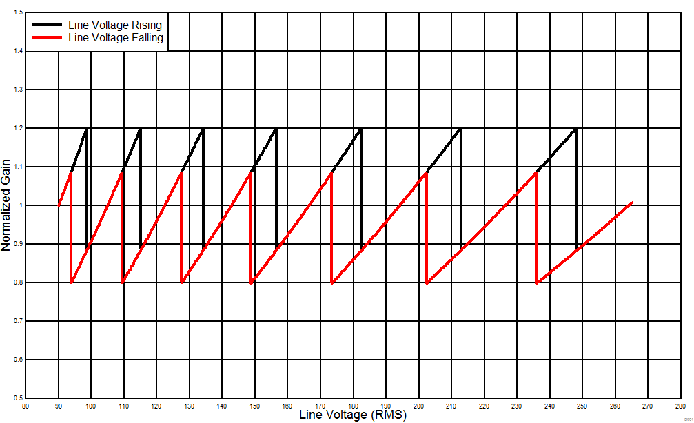
UCC28056 D001_SLUSD37.gifFigure 20. Normalized Gain vs Line Voltage