SLUSD37E October 2017 – November 2019 UCC28056
PRODUCTION DATA.
- 1 Features
- 2 Applications
- 3 Description
- 4 Revision History
- 5 Device Comparison Tables
- 6 Pin Configuration and Functions
- 7 Specifications
-
8 Detailed Description
- 8.1 Overview
- 8.2 Functional Block Diagram
- 8.3
Feature Description
- 8.3.1 CrM/DCM Control Principle
- 8.3.2 Line Voltage Feed-Forward
- 8.3.3 Valley Switching and CrM/DCM Hysteresis
- 8.3.4 Transconductance Amplifier with Transient Speed-up Function
- 8.3.5 Faults and Protections
- 8.3.6 High-Current Driver
- 8.4 Controller Functional Modes
- 9 Application and Implementation
- 10Power Supply Recommendations
- 11Layout
- 12Device and Documentation Support
- 13Mechanical, Packaging, and Orderable Information
8.3.3 Valley Switching and CrM/DCM Hysteresis
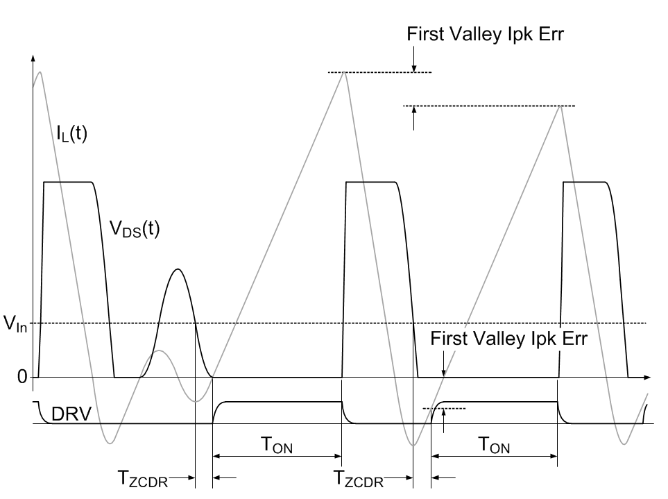
The UCC28056 controller achieves maximum efficiency enabling power switching operation when the drain voltage of the MOSFET is at a minimum (sometimes referred to as valley), of the resonance that occurs during the TDCM period . Any energy stored in the Drain node capacitance (CDE ) dissipates in the power switch during its turnon transition time. Valley switching ensures minimum energy is stored in CDE prior to the turnon period and hence minimum switching loss. After the TDCM period, the controller waits for the next available valley on the drain voltage before initiating a new switching cycle. The actual TDCM duration is therefore always an integer multiple of the drain resonance period. If the calculated TDCM period extends over a valley boundary the actual TDCM duration steps up in value by one resonant period. This step change in TDCM duration causes a step change in Line current that rapidly decays as the TON(θ) computation iterates to a new solution to reflect the step change in TDCM duration. Line current distortion, resulting from valley transitions, is kept to a minimum by computing the TDCM duration from the COMP voltage. The COMP voltage varies little over the period of a Line cycle and hence the calculated TDCM duration changes very little over the period of a Line cycle.
Line current distortion is particularly severe during the transition from the first valley (CrM) to the second valley (DCM) operation while the input voltage is low. In this region, the first valley duration is extended by the clamping action of the power switch body diode. In this region Line current is reduced when switching on the first valley, (CrM) , because the inductor current is negative at the start of the on period. The reduction in Line current is not observed for second or subsequent valley (DCM) operation because the inductor current starts the on period from zero. UCC28056 implements hysteresis in the TDCM computation to virtually eliminate the possibility of repeated CrM/DCM transitions across a Line cycle. Such transitions can only occur if the twice Line frequency ripple on the COMP voltage is greater than 12% at the CrM/DCM boundary.
 Figure 21. Drain Voltage and Inductor Current Transitioning from DCM to CrM