SLUUBG8C November   2018  – October 2021


  1.   Trademarks
  2. 1 Introduction
  3. 2 Description
  4. 3 Features
    1. 3.1 I/O Description
    2. 3.2 Jumpers (Shunt) Setting
  5. 4 Electrical Specifications
  6. 5 Test Summary
    1. 5.1 Definitions
    2. 5.2 Equipment
      1. 5.2.1 Power Supplies
      2. 5.2.2 Function Generators
    3. 5.3 Equipment Setup
      1. 5.3.1 DC Power Supply Settings
      2. 5.3.2 Digital Multi-Meter Settings
      3. 5.3.3 Two-Channel Function Generator Settings
      4. 5.3.4 Oscilloscope Setting
      5. 5.3.5 Jumper (Shunt) Settings
      6. 5.3.6 Bench Setup Diagram
  7. 6 Power-Up and Power-Down Procedure
    1. 6.1 Power Up
    2. 6.2 Power Down
  8. 7 Test Waveforms (CL=0pF) With Different DT Configurations
    1. 7.1 DT Connected to VCCI (J-DT Option B in Table 1-1 )
    2. 7.2 DT Pin Floating or Left Open (J-DT Option A in Table 1-1 )
    3. 7.3 DT Pin Connected to RDT (J-DT Option C in Table 1-1 )
  9. 8 Schematic
  10. 9 Layout Diagrams
  11. 10List of Materials
  12. 11Revision History

Schematic

Figure 8-1 only shows the schematic diagram for UCC21520EVM. The schematic diagrams for the UCC20520EVM, UCC21521CEVM, and UCC21530EVM are similar to Figure 8-1, with the exception that the device under test (U1) could be in one of the following driver ICs: UCC21520DW, UCC20520DW, UCC21521CDW, or UCC21530DWK.
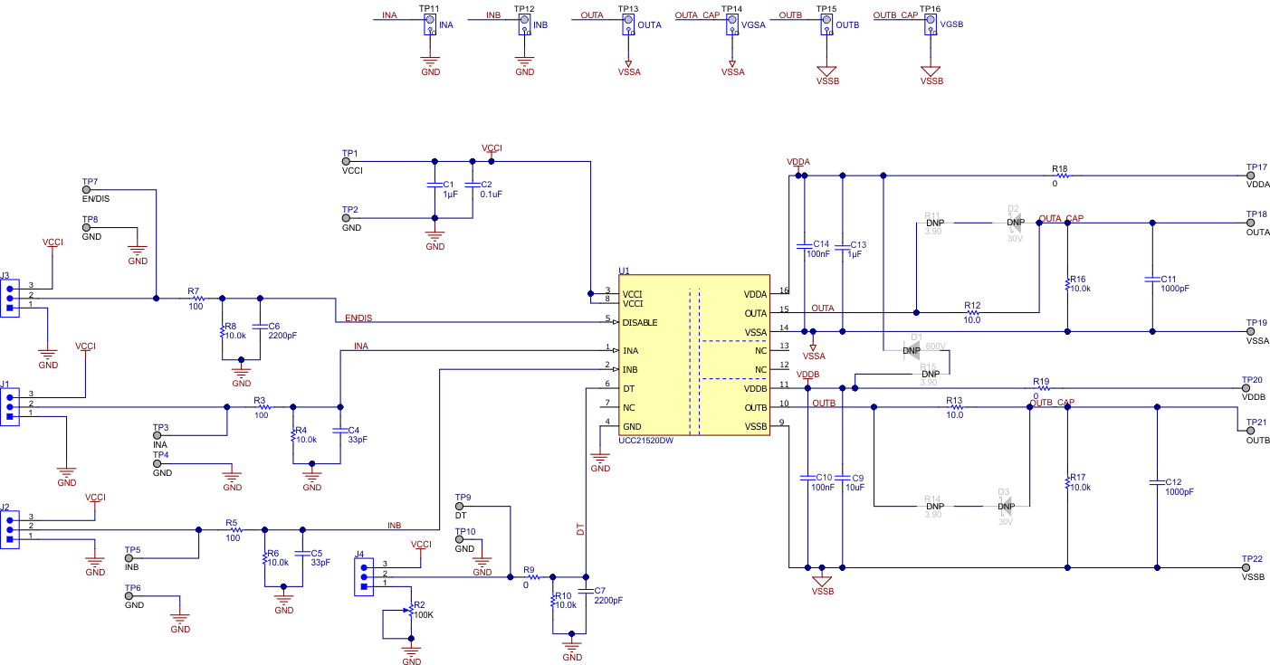
GUID-20210429-CA0I-TP7L-RNTP-J3LMHS40DNGT-low.gifFigure 8-1 UCC21520EVM-286 Schematic