SLUUCF7
April 2021
Trademarks
1
Introduction
1.1
EVM Features
1.2
I/O Descriptions
2
Test Summary
2.1
Equipment
2.2
Equipment Setup
2.3
Software Setup
2.4
Test Procedure
2.4.1
Initial Settings
2.4.2
Communication Verification
2.4.3
Switched Cap Mode Charge Verification
2.4.4
Bypass Mode Charge Verification
2.4.5
Dual BQ25960 Operation
2.4.6
BQ25611D Charge Verification
3
PCB Layout Guidelines
4
Board Layout, Schematic, and Bill of Materials
4.1
Board Layout
4.2
Schematic
4.3
Bill of Materials
4.2
Schematic
Figure 4-9
through
Figure 4-11
illustrate the schematic for the BQ25960EVM.
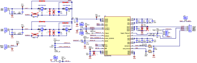
Figure 4-9
BQ25960EVM Schematic (Page 1)
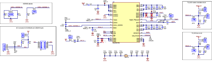
Figure 4-10
BQ25960EVM Schematic (Page 2)
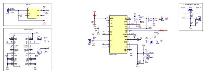
Figure 4-11
BQ25960EVM Schematic (Page 3)