SLUUCH6B september 2022 – september 2023 TPS543B22
- 1
- Abstract
- Trademarks
- 1Introduction
- 2Configurations and Modifications
-
3Test Setup and Results
- 3.1 Input/Output Connections
- 3.2 Efficiency
- 3.3 Output Voltage Regulation
- 3.4 Load Transient and Loop Response
- 3.5 Output Voltage Ripple
- 3.6 Input Voltage Ripple
- 3.7 Synchronizing to a Clock
- 3.8 Start-up and Shutdown with EN
- 3.9 Start-up and Shutdown with VIN
- 3.10 Start-up Into Pre-Bias
- 3.11 Hiccup Current Limit
- 3.12 Thermal Performance
- 4Board Layout
- 5Schematic and Bill of Materials
- 6Revision History
3.7 Synchronizing to a Clock
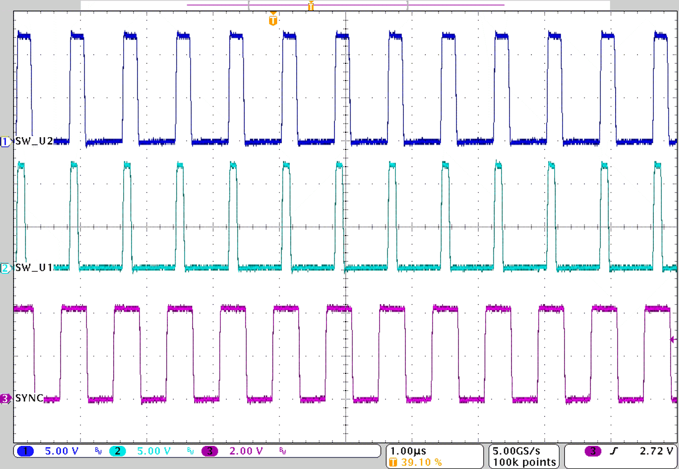
Figure 3-19 shows U1 and U2 synchronized to an external clock of 1.25 MHz at the SYNC test point. To synchronize to the clock at the SYNC test point, place a shunt on the ENSYNC_U1 or ENSYNC_U2 jumper or jumpers to enable the output of the buffers.
Figure 3-20 shows the transitions to and from synchronizing to an external clock with 20-A load. 16 pulses with a frequency of 1-MHz were sent to the SYNC testpoint on the EVM. In this waveform, after four pulses, the TPS543B22 begins synchronizing to the clock. After the clock goes away, the TPS543B22 switches at 70% of the internal clock frequency for four pulses then transitions back to the normal internal clock frequency. There is only a small variation in the output voltage during these transitions.
 Figure 3-19 U1 and U2 Synchronized to
a Clock
 Figure 3-20 U2 Clock Synchronization
Transitions