SLUUCH6B september 2022 – september 2023
- 1
- Abstract
- Trademarks
- 1Introduction
- 2Configurations and Modifications
-
3Test Setup and Results
- 3.1 Input/Output Connections
- 3.2 Efficiency
- 3.3 Output Voltage Regulation
- 3.4 Load Transient and Loop Response
- 3.5 Output Voltage Ripple
- 3.6 Input Voltage Ripple
- 3.7 Synchronizing to a Clock
- 3.8 Start-up and Shutdown with EN
- 3.9 Start-up and Shutdown with VIN
- 3.10 Start-up Into Pre-Bias
- 3.11 Hiccup Current Limit
- 3.12 Thermal Performance
- 4Board Layout
- 5Schematic and Bill of Materials
- 6Revision History
4.1 Layout
The board layout for the TPS543B22EVM is shown in Figure 4-1 through Figure 4-12. The top-side layer of the EVM is laid out in a manner typical of a user application. The top, bottom, and internal layers are 2-oz. copper. The small size U1 circuit takes up an area of only approximately 275 mm2 as shown on the silkscreen.
All of the required components for the TPS543B22 are placed on the top layer for U1. The input decoupling capacitors, VDRV capacitor, VCC capacitor, and bootstrap capacitor are all located as close to the IC as possible. Additionally, the voltage set point resistor divider components are kept close to the IC. An additional input bulk capacitor is used near the input terminal to limit the noise entering the converter from the supply used to power the board. Critical analog circuits such as the voltage set point divider, EN resistor, MODE resistor, and FSEL resistor are kept close to the IC and terminated to the quiet analog ground (AGND) island on the top layer.
The top layer contains the main power traces for VIN, VOUT, and SW. The top layer power traces are connected to the planes on other layers of the board with multiple vias placed around the board. There are multiple vias near the PGND pins of the IC to help maximize the thermal performance. Each TPS543B22 circuit has their own dedicated ground are for quiet analog ground that is connected to the main power ground plane at a single point. This single point connection is done on the internal ground planes. Lastly the voltage divider network ties to the output voltage at the point of regulation, the copper VOUT area on the top layer.
The mid layer 1 is a large ground plane and an analog ground island for the MSEL and FSEL resistor and VCC capacitor to connect to by vias. minimize cuts in the ground plane. The U1 VOUT has a large copper pour for carrying the output current. The input bus for the 2nd filter connects on the mid layer 1 from the VOUT of U2 to the 2nd stage filter using vias.
The mid layer 2 has VIN copper area beneath each IC to connect the VIN pins together with a low impedance connection. Lastly, the remaining area of this layer is filled in with PGND and additional copper plane for the 2nd stage filter. The mid layer 3 and mid layer 4 is mostly a power ground plane with minimal trace and cuts.
The bottom layer is primarily used for another ground plane. This layer also has an additional VOUT copper area for the U2 circuit. Lastly, the load transient circuit is placed on this side of the EVM.
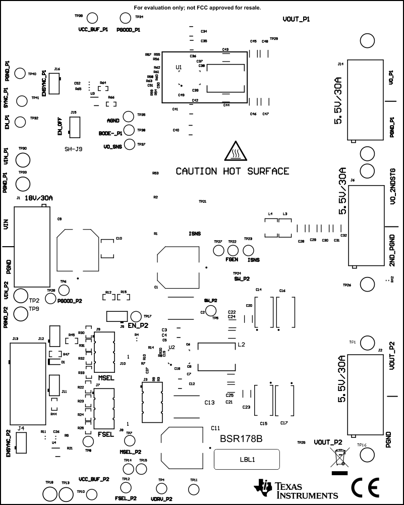 Figure 4-1 Top Overlay
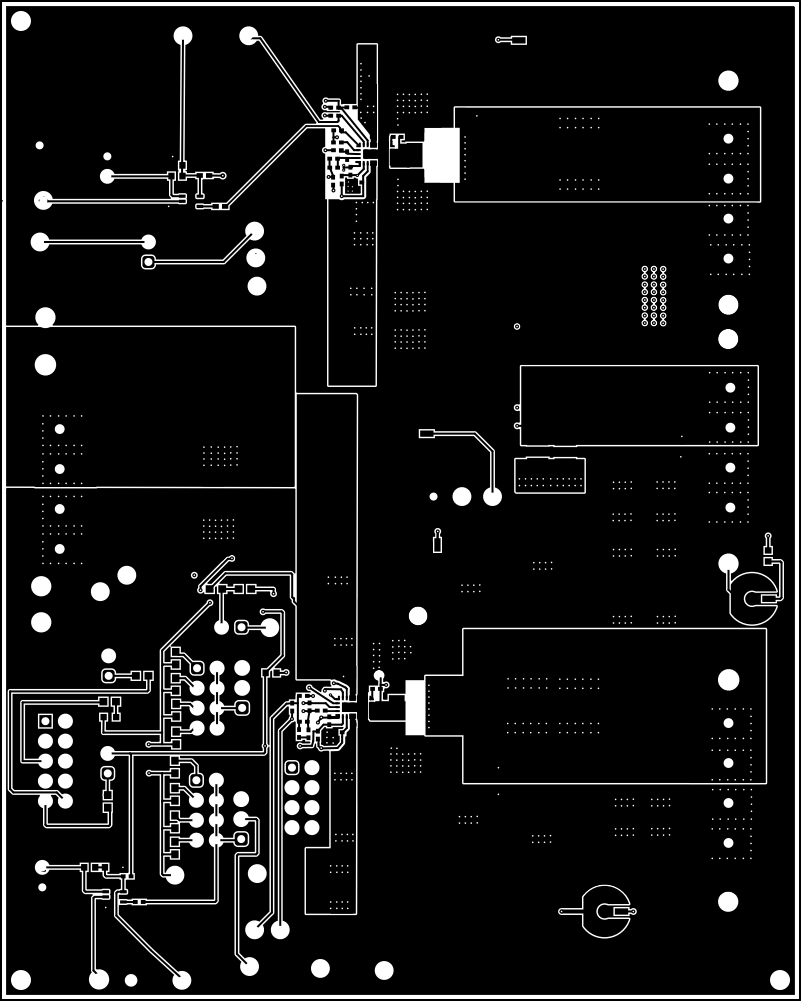 Figure 4-3 Top Layer
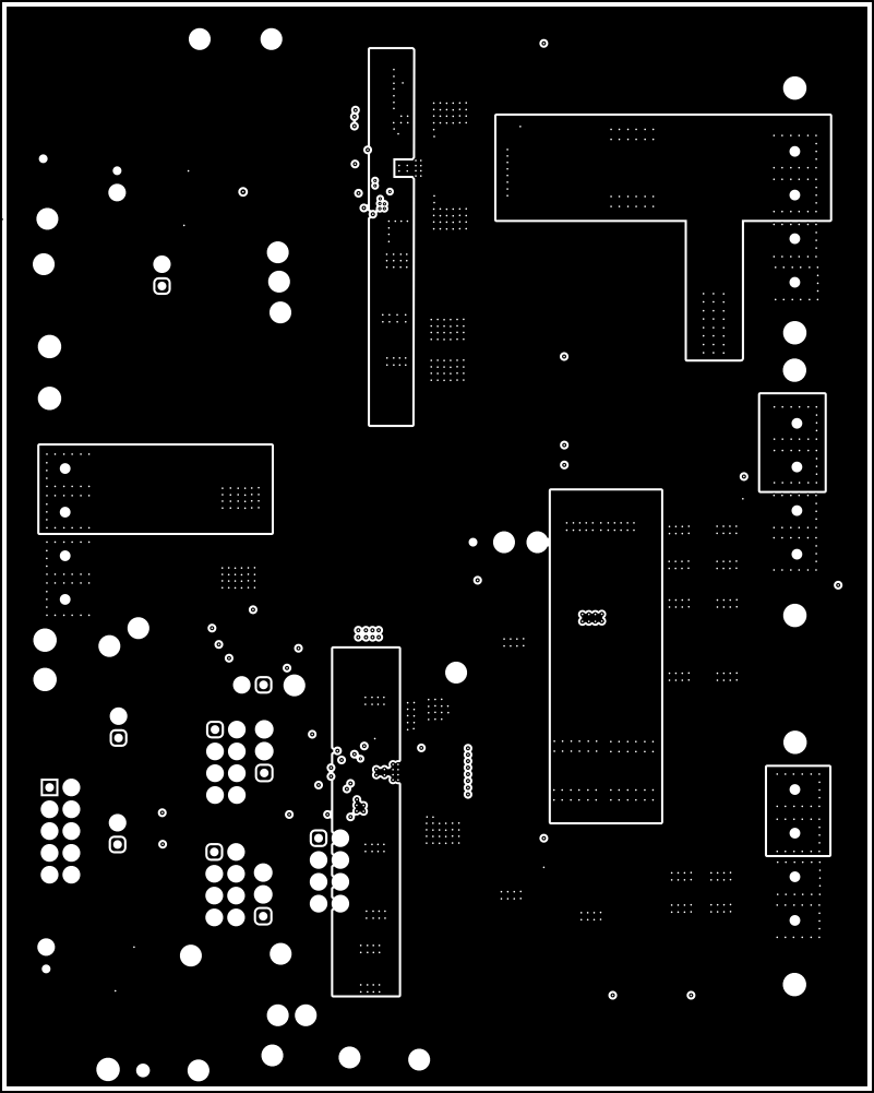 Figure 4-5 Signal 2
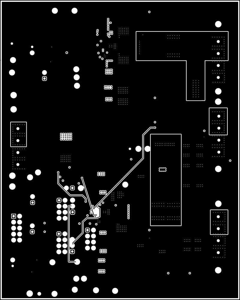 Figure 4-7 Signal 4
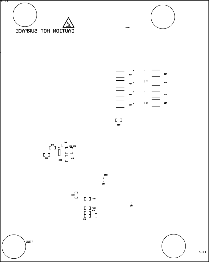 Figure 4-9 Bottom Overlay
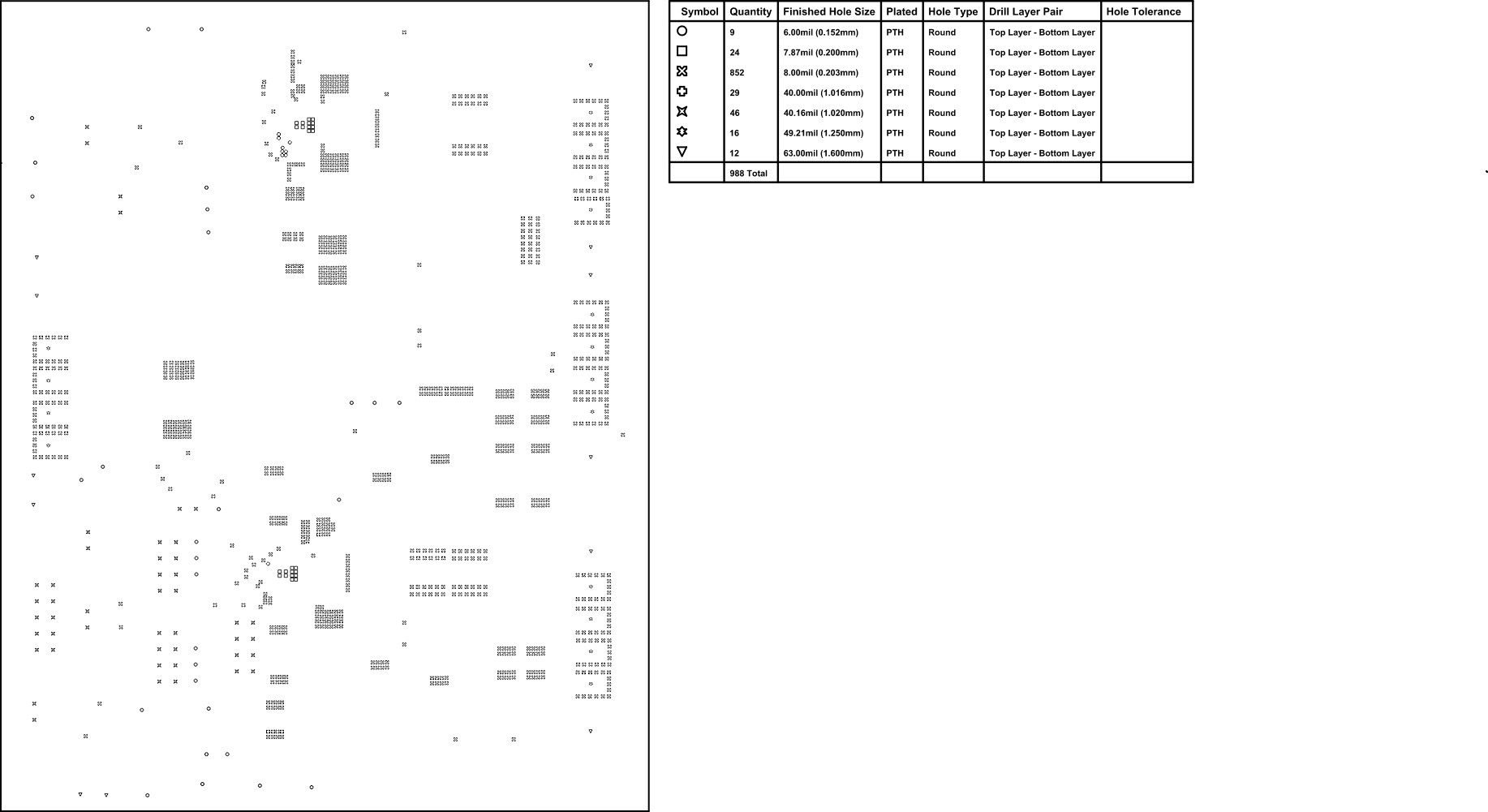 Figure 4-11 Drill Drawing
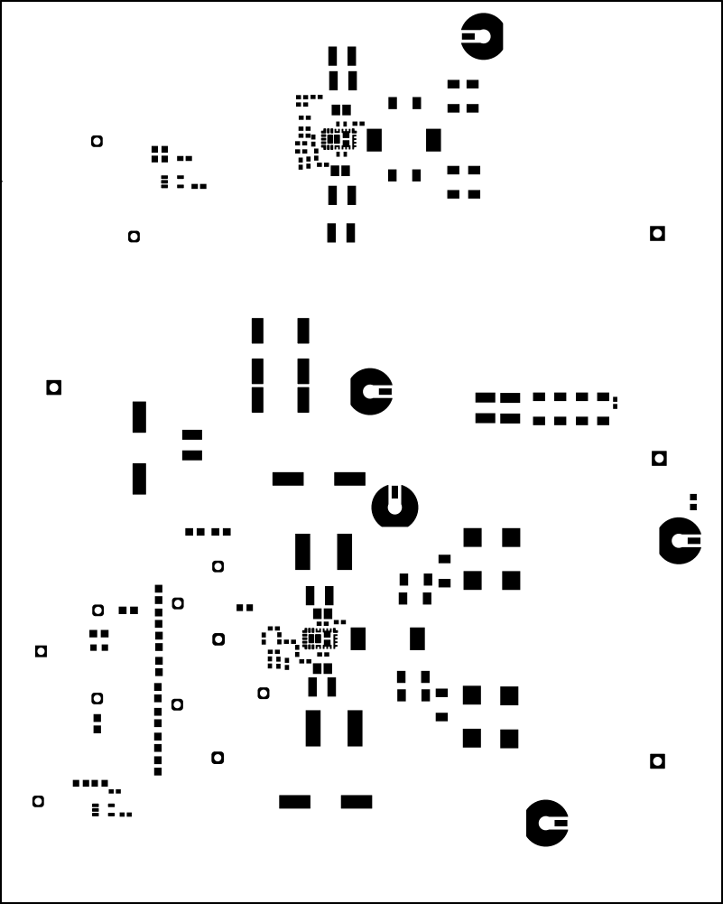 Figure 4-2 Top Solder
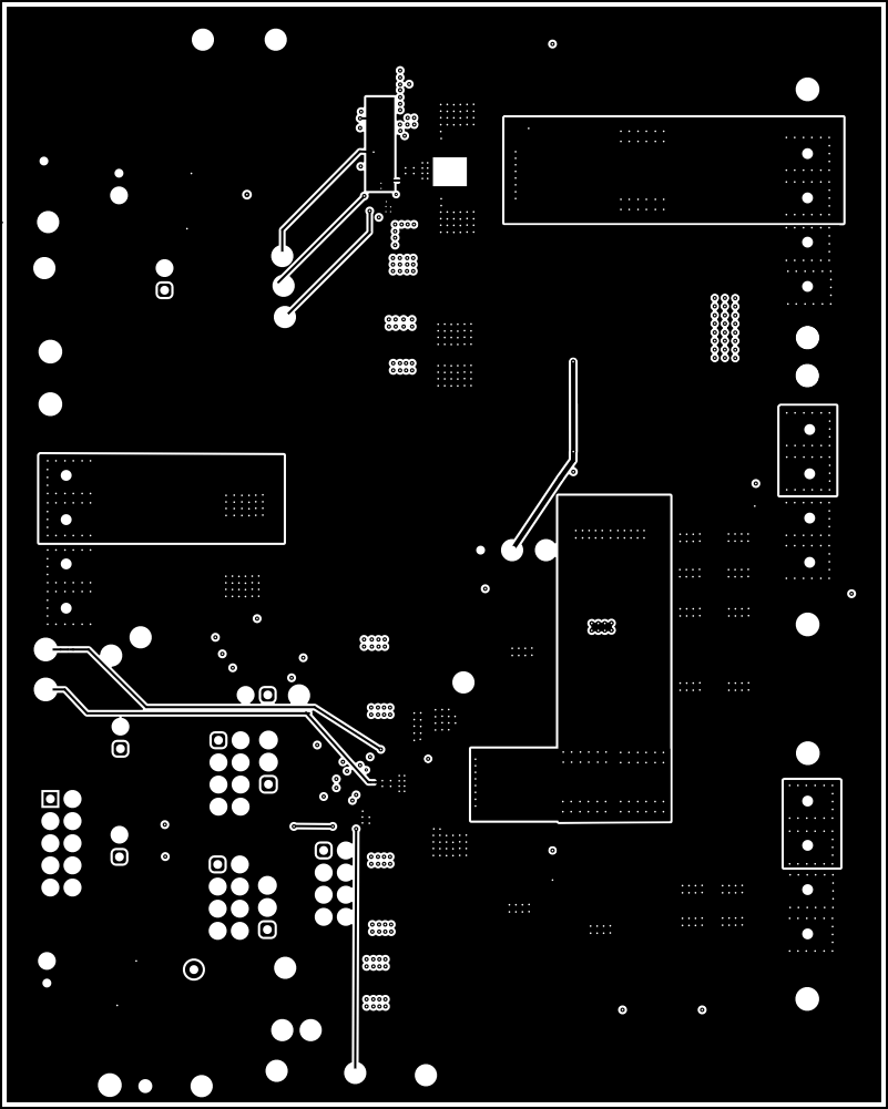 Figure 4-4 Signal 1
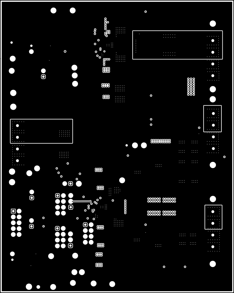 Figure 4-6 Signal 3
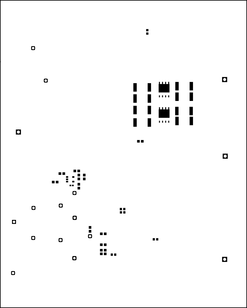 Figure 4-8 Bottom Solder
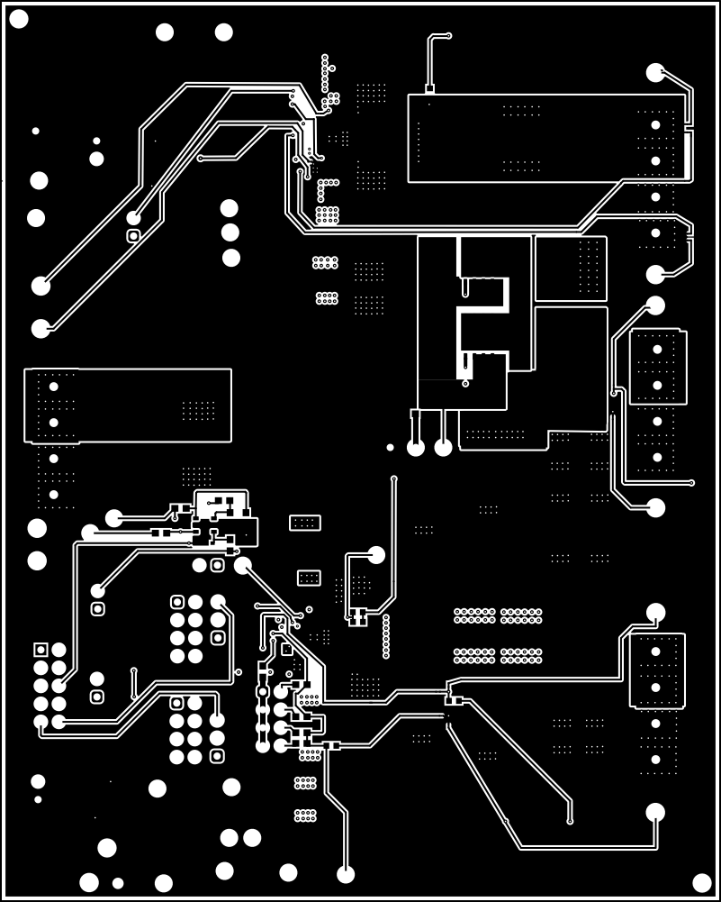 Figure 4-10 Bottom Layer
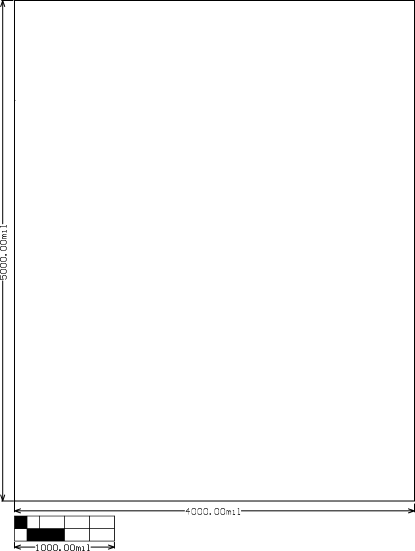 Figure 4-12 Board Dimensions