SLVA321A August 2011 – April 2021 DRV8811 , DRV8818 , DRV8821 , DRV8823 , DRV8823-Q1
2.1 Fast Decay
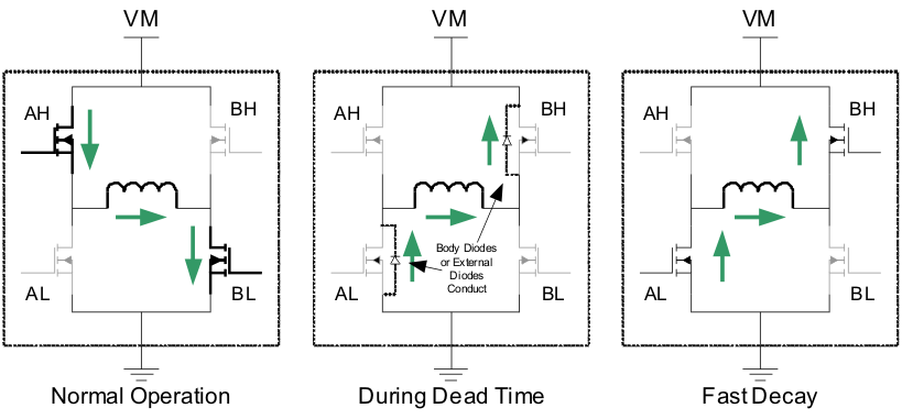
During a fast decay recirculation mode, current is said to decay towards zero as fast as possible. This is attained by disabling the energizing FET switches and then enabling the opposing FET switches (synchronous decay), or letting current flow through free wheeling diodes (asynchronous decay).
Current decays the fastest possible because a voltage of greater magnitude but opposing polarity is applied to the inductive load.
On synchronous decay, the proper technique to achieve fast decay mode is to employ a break before make mechanism in order to avoid shoot through. If the opposing FETs are enabled as soon as the energizing FET switches are disabled, there will be a short period of time in which all four FET switches will conduct. This is extremely hazardous to the device.
The solution is to add a period of time in which all FET switches are off, called dead time. During this time, energizing FET switches are allowed to switch to their OFF state and inductive load existing current is carried by either body diodes or external Schotky diodes.
H Bridges employing asynchronous decay will let the diodes conduct the current while it decays.
H Bridges employing synchronous decay will turn the opposing FET switches until current decays down to zero, or a fixed time off elapses.
 Figure 2-1 Fast Decay Mode
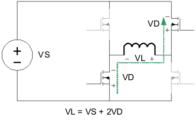
Note that the voltage applied to the inductive load is that of the source plus two diode forward voltage drops, or current multiplied by respective switch RDSon.
 Figure 2-2 Voltage Applied to the Inductive Load