SLVA997A November 2018 – July 2021 TPS61322
2 Single Pulse Power Save Mode Control Scheme
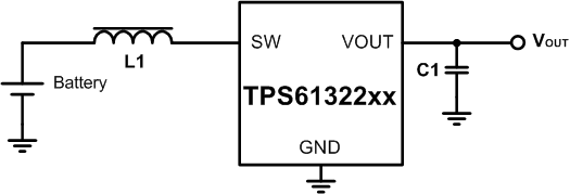
The TPS61322xx is a low quiescent, high efficiency synchronous boost converter family based on hysteretic current control topology. The TPS61322xx is designed for systems which need a constant on and quiet power rail. The input source can be one cell alkaline battery, CR2032, and lithium battery. Figure 2-1 shows the typical application schematic of TPS61322xx.
 Figure 2-1 Single Pulse Control Scheme
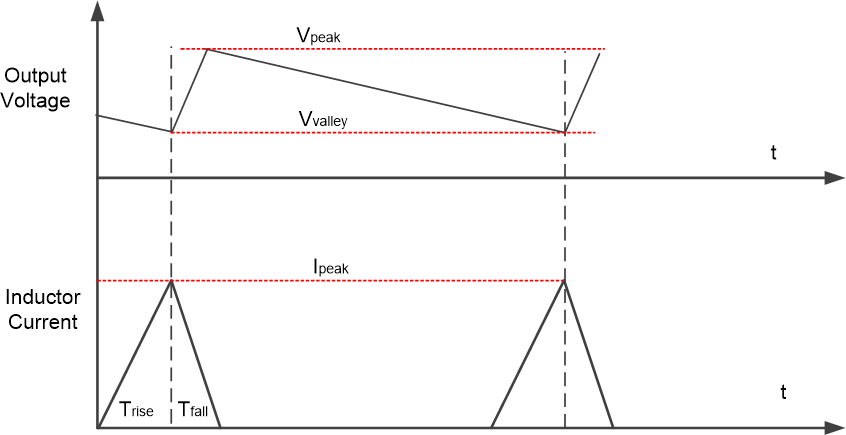
The TPS61322xx uses single pulse power save mode and keeps the output voltage the same over all the load range. The typical control scheme is shown in Figure 2-2
 Figure 2-2 Single Pulse Control Scheme
There are 3 operation subintervals for TPS61322xx at light load: on-phase, off-phase and stop-phase. During on-phase, the low-side MOSFET is ON and high-side MOFET is OFF, the input source charges the inductor and the subsystem is powered by the output capacitor. The inductor current ramps up until triggers the hysteresis current Ihys, then the on-phase ends and the off-phases starts. During off-phase, the low-side MOSFET is OFF and high-side MOSFET is ON. The inductor charges the output capacitor and powers the sub-system at the same time. The inductor current ramps down until trigger zero current, then the stop-phase starts. During stop-phase, both low-side and high-side MOSFET are OFF and all the energy is from the output capacitor. The internal control loop is always active and regulate the stop-phase time.
This control scheme helps reduce the output capacitor significantly because only one current pulse is output in each power save mode cycle.