SLVAEN1A February 2020 – November 2022 TPS61022 , TPS61023
2 Proposed Circuit Principle
The proposed solution utilizes a special feature of the EN logic threshold voltage, as shown in Table 2-1:
- When VIN > 1.8 V or VOUT > 2.2 V, the EN logic high threshold VEN_H is 1.2 V.
- After the device starts to operate, the typical EN logic low threshold VEN_L is typically 0.42 V, with a minimum of 0.35 V and a maximum of 0.42 V
| Parameter | Test Condition | MIN | TYPICAL | MAX | Unit | |
|---|---|---|---|---|---|---|
| VEN_H | EN logic high threshold | VIN > 1.8 V or VOUT > 2.2 V | 1.2 | V | ||
| VEN_L | EN logic low threshold | VIN > 1.8 V or VOUT > 2.2 V | 0.35 | 0.42 | 0.45 | V |
Figure 2-1 shows a simplified schematic of the proposed solution. The operating principle details follow:
- At the beginning, the device VIN < 1.7 V and VOUT = 0 V. The device shuts down and disconnects VIN and VOUT. The NMOS Q1 turns off and the voltage at EN pin VEN is equal to VIN.
- When VIN increases to higher than a typical 1.7 V (maximum 1.8 V) and EN voltage is higher than the logic high threshold, the device starts to operate. The EN logic high threshold is typically 0.95 V with a maximum value of 1.2 V. As VEN = VIN > 1.7 V, the device begins the soft-start process. During the soft-start process, the device initially pre-charges the VOUT closed to VIN, then switches to boost the output to the higher voltage.
- After the VOUT becomes higher than 2.2 V, the UVLO value of the VIN pin is changed to typical 0.4 V and the EN logic low threshold is changed to 0.42 V. Because of the R5, R6, and C2, the Q1 gate voltage is still too low to turn on, the VEN is still equal to VIN.
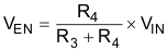
- After the VOUT ramps to the setting value and Q1
turns on, the voltage at the EN pin is defined by Equation 1. Equation 1.
- If VIN declines and results in VEN lower than typical 0.42 V, the device shuts down. The VOUT is discharged by the loading. After Q1 turns off, VEN will be equal to VIN again. However, the device would keep off if VIN < 1.7 V.
 Figure 2-1 Schematic of the Proposed
Circuit
Figure 2-1 Schematic of the Proposed
CircuitBased on the previous analysis , the UVLO value set by this method must be lower than 1.7 V.
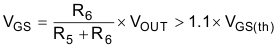
The function of the R5, R6, and C2 is to keep Q1 off before the VOUT is ready. But Q1 must turn on after the output voltage is stable at the setting voltage. The gate-to-source voltage at stable condition is defined by Equation 2, which should be 10% higher than the MOSFET gate to source threshold voltage for design margin.
where
- VGS(th) is the gate-to-source threshold voltage of a MOSFET
- VOUT is the setting value of the output voltage
The time constant of the R5, R6, and C2, which is defined by Equation 3, is suggested to be the startup time of the device – 700 µs (typical).

Figure 2-2 shows the method to shut down the boost converter through an external control logic pin. The device shuts down if CTRL is high, while the device is controlled by the proposed circuit if CTRL is low. If the CTRL signal can support open-drain output, it can connect to the EN pin directly. Then the boost is off at CTRL low logic, and it is controlled by the proposed circuit at CTRL open-drain.
 Figure 2-2 Method to Shutdown Proposed
Circuit With I/O
Figure 2-2 Method to Shutdown Proposed
Circuit With I/OAssuming the output voltage is set to 5 V and the new UVLO voltage is 1.2 V, the following process details the design of the components for the proposed circuit:
- Set R3 to be 1 MΩ, R4 will be 538 kΩ based on Equation 1. Considering the threshold variation in Table 2-1, the new UVLO value would have a 1-V minimum and 1.29-V maximum.
- Select CSD13381F4 as the Q1, which has a typical 0.85-V gate-to-source threshold voltage VGS(th) with a 0.65-V minimum and 1.1-V maximum at room temperature. Considering the variation of VGS(th) overtemperature, the gate-to-source voltage must be higher than 1.2 V to safely turn on the MOSFET. Select 1-MΩ R5, the R6 would be 359 kΩ according to Equation 2.
- Select the time constant of the R5, R6, and C2 to be 700-µs (TPS61022 start up time), the C2 would be 2.6 nF from Equation 3.
Figure 2-3 shows the value of the external components.
 Figure 2-3 Components Value of the
Proposed Circuit
Figure 2-3 Components Value of the
Proposed Circuit