SLVAF11 June 2021 TPS51397A , TPS566231 , TPS566235 , TPS566238 , TPS568230
3.1 Limits of Output Capacitance
In buck converters, the slope of open loop gain can be seen as -40dB/decade after double poles frequency ω0. When the ripple injection zero frequency ωRI is smaller than bandwidth, the loop gain will cross 0dB with -20dB/decade slope, as shown in Figure 3-1. Otherwise, it will cross 0dB with -40dB/decade slope, as shown in Figure 3-2.
 Figure 3-1 Loop Gain of D-CAP2 Converter with -20dB/Decade at 0dB
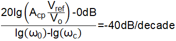
Assuming the loop gain drops with -40dB/decade slope after ω0, the cross frequency at 0dB is denoted as ωc. From Figure 3-1 and Figure 3-2, it’s known that Equation 7 is needed for a -20dB/decade cross.

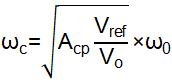
To calculate the frequency ωc, we can first get Equation 8 with ωc
Then ωc can be derived as:
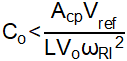
Substituting Equation 4 and Equation 9 into Equation 7, Equation 10 can be derived to ensure -20dB/decade cross.
If further considering the DCR of inductor rL, Equation 10 will become:
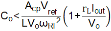
Since the inductance L is normally designed with the target to let inductor current ripple be about 20%-40% of max load current rating. With Equation 10 or Equation 11, the upper limit of capacitance value can be got for loop stability.
In D-CAP2/D-CAP3 control, Acp and ωRI are the parameters determined by the internal circuit inside converters. Table 3-1 shows the Acp and ωRI of some devices with D-CAP2 or D-CAP3 control.
| Device | Acp | ωRI (fsw=600kHz) |
|---|---|---|
| TPS568230 | 29.3 | 270krad/s (43kHz) |
| TPS566235 | 29.36 | 198krad/s (31.5kHz) |
| TPS566231 | 36 | 247krad/s (39.3kHz) |
Note: ωRI is already given in some data sheets (sometimes named as time constant, it's the reciprocal of ωRI). Acp of a device can be estimated by checking the gain before double poles, which equals to 20lg(Acp*Vref/Vo)dB in bode plot.
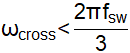
From Equation 11, it can be found that smaller output capacitor tends to bring a -20dB/decade cross. But too small output capacitance will make the double poles frequency too high and increase the bandwidth a lot. That may also cause insufficient phase margin, since the phase will drop apparently at high frequency range due to the effects of delay factor. For D-CAP2/D-CAP3 mode converter, normally the bandwidth needs to be limited below 1/3*fsw. That corresponds to a lower limit for output capacitance.
To get the limit, first we can get the loop gain at ripple injection zero in Figure 3-1 as:
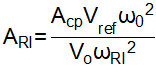
Loop gain will drop with -20dB/decade slope from ARI and cross 0dB at ωcross:
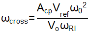
Limit the crossover frequency below 1/3*fsw and the lower limit of output capacitance can be derived as Equation 15.
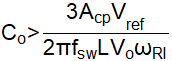
Above all, the Equation 11 and Equation 15 are the upper limit and lower limit of output capacitance for loop stability.