SLVAF59 April 2021 TPS2372 , TPS2373 , TPS23730 , TPS23731 , TPS23734 , TPS2375 , TPS2375-1 , TPS23750 , TPS23751 , TPS23752 , TPS23753A , TPS23754 , TPS23754-1 , TPS23755 , TPS23756 , TPS23757 , TPS23758 , TPS2376 , TPS2376-H , TPS2377 , TPS2377-1 , TPS23770 , TPS2378 , TPS2379
3.2 Primary Side of the DCDC
The primary side of the DCDC is the left side of the transformer. Most PoE designs use flybacks or active clamp forward topologies to achieve isolation. Typically, the primary side is very similar between designs because the input voltage and power levels are very consistent. With EVM’s and reference designs, if there is one already determined for the power level (example, 51W), then the input current and voltage and therefore power are always going to be the same. Copying an EVM minimizes risk for proper operation.
Input Bulk Capacitor: PoE requires an input bulk capacitor to provide enough energy for the DCDC. This capacitor requires ESR – preferably this is an electrolytic cap. However, ceramics can be used, but a 1 ohm resistor between the cap bank and RTN is strongly recommended for startup. The bulk capacitance is good in helping with transients (voltage spikes). It is important to have. The bulk capacitor is recommended to be within the following range for the appropriate power level as shown in Table 3-1.
| Power | Bulk Cap |
|---|---|
| 13W | 10-22uF |
| 25W | 33-47uF |
| 50W | 68-100uF |
| 70W | 100uF-200uF |
 Figure 3-5 Input Bulk Capacitor
Input Filter. This filter is technically optional but it is strongly suggested. These are the smaller capacitors and inductor on VDD-RTN. These help reduce input ripple and therefore output ripple. There is no requirement here, so the inductor is not required. An inductor can be chosen to not be included in the design, but these capacitors are pretty much needed. These capacitors need to be ceramic. They can be a combination with electrolytic, but then the ripple ratings become an important factor in electrolytic. The Designing with the TPS23753 Powered-Device and Power Supply Controller application note includes a section on the calculation for the input inductor and caps. See section 2.7.4
 Figure 3-6 Input Filter
VCC power: The IC input power is actually VCC not VDD. So VCC should be connected to the auxiliary winding of the transformer, with some rectification and appropriate capacitance to power the IC. If using the TPS2373x, only a 1uF is required thanks to advanced startup. If using the TPS2375x, (except TPS23755 and TPS23758), something like 22uF is required, preferably electrolytic. Sometimes higher capacitance is needed in active clamp forwards (ACF) for the TPS2375x parts. If a ceramic capacitor is used, please note the effective capacitance needs to be 22uF; so please include the derided value. This is why capacitor type, size, voltage rating and placement are important. Something else to note is that if VCC is powering anything other than the IC, that will drain the capacitor and therefore must be accounted for. As is apparent, essentially every part and power level is different, so please see an EVM for best practice. Active clamp forwards usually have two diodes and an inductor to minimize the ripple. At a minimum 1mH is used but we recommend a 2.2mH inductor.
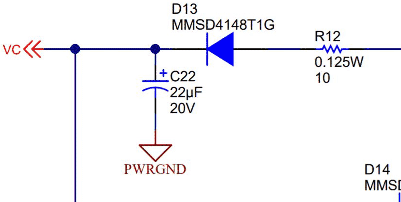 Figure 3-7 VCC Input: Flyback
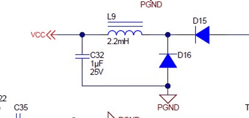 Figure 3-8 VCC Input: Active Clamp Forward
Primary side regulation designs will also require an additional cap and resistor. These are there to reduce peak charging since this is used in the feedback loop. What is used in TI designs is the optimal solution.
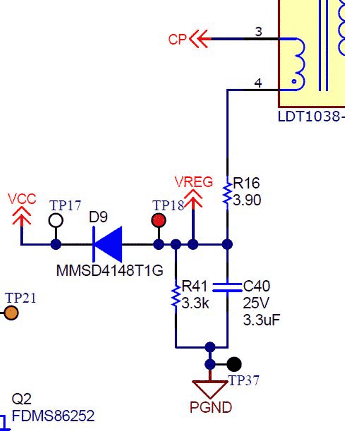 Figure 3-9 VCC Input: PSR Flyback
Primary side FET(s). There are two if it is an active clamp. The VDS should be 150V. The gate charge should be as low as possible, using the EVM or Reference design MOSFET choice as a baseline. The package of the MOSFET should be at least QFN-8, but certainly not SOT-23. The primary current depends on the primary inductance of the transformer and input power, but usually 2A-3A. For example, the TPS23730EVM-093 is a 51W ACF, and it uses a 3A rated MOSFET. If there is an active clamp, there needs to be an active clamp capacitor -- rated for 250V and usually 0.047uF. This helps set the resonance for the active clamp, so this usually does not need to be changed. The active clamp FET is P-Type and requires similar VDS as the N-FET. The FETs sometimes require pull down circuitry. This is either a diode, or a diode, BJT and resistor. The later is the fastest option. Essentially, the best thing to do is to copy a reference design OR prepare space for all of the options. Additionally, the FET needs a resistor on the gate to slow down the turn on time. This resistor is recommended between 4-50 ohms. If the resistance is too high, it can cause timing issues, but the main concern is that it decreases efficiency.
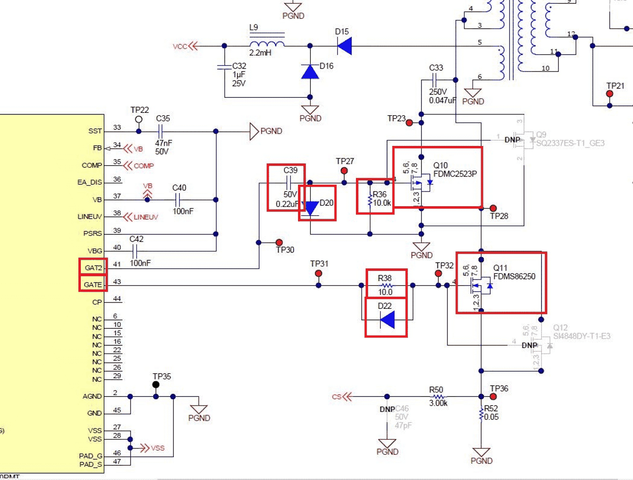 Figure 3-10 Primary MOSFETs: Active Clamp Forward
Current Sense: the current sense resistor is the <1ohm resistor on the source of the primary FET. Ensure this is a large package (at least 1206).The resistance value and power level can be calculated from primary inductance and primary current. Additionally, always leave room for slope compensation. This is a resistor in series with the CS pin and another capacitor. This capacitor provides filtering, but it is not recommended to go above 100pF. This will round off the signal, which makes it difficult to compensate. A good rule is the RC corner frequency created by the resistor and capacitor should be no less than 10x the switching frequency. The resistor is typically 1K-5K ohms for ACFs, and around 1K for flybacks. Please see the reference design for best practice and fine-tuned results. Sometimes a feed forward resistor is used as well.
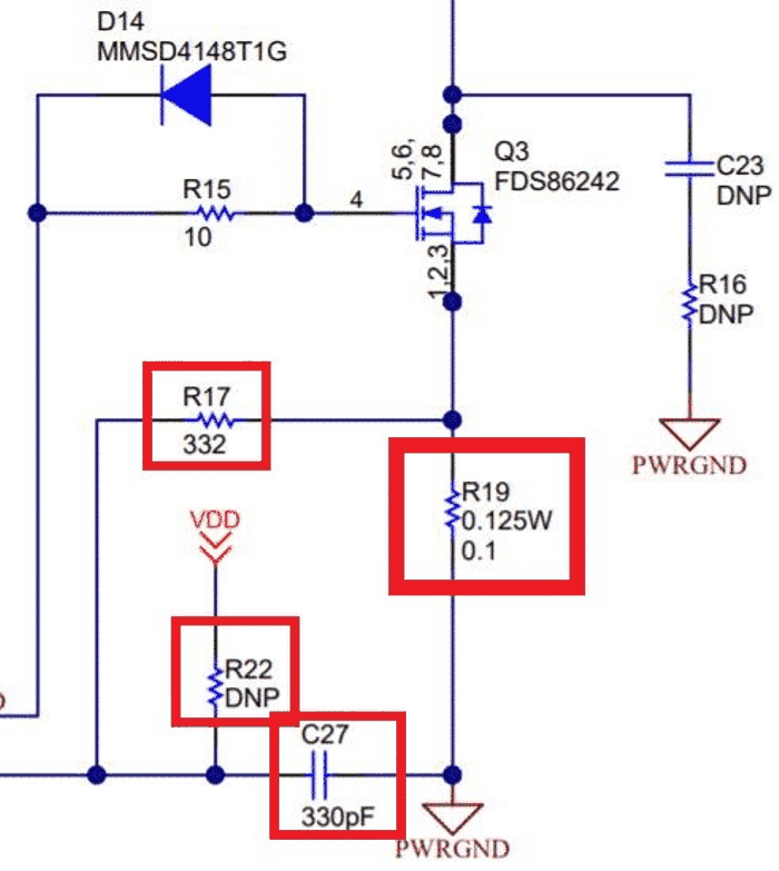 Figure 3-11 Current Sense and Slope Compensation
Primary FET clamp: If it is a flyback, the primary side needs a clamp.The diode needs to be fast enough to handle the transient (reverse recovery time of 25-50ns). Ensure these components can handle the power going through them. Please note, the TI Power Stage Designer Tool has a specific section for the RCD Snubber Calculation. A TVS diode can be used instead of the resistor and capacitor. The same principles apply of speed, power and voltage ratings.
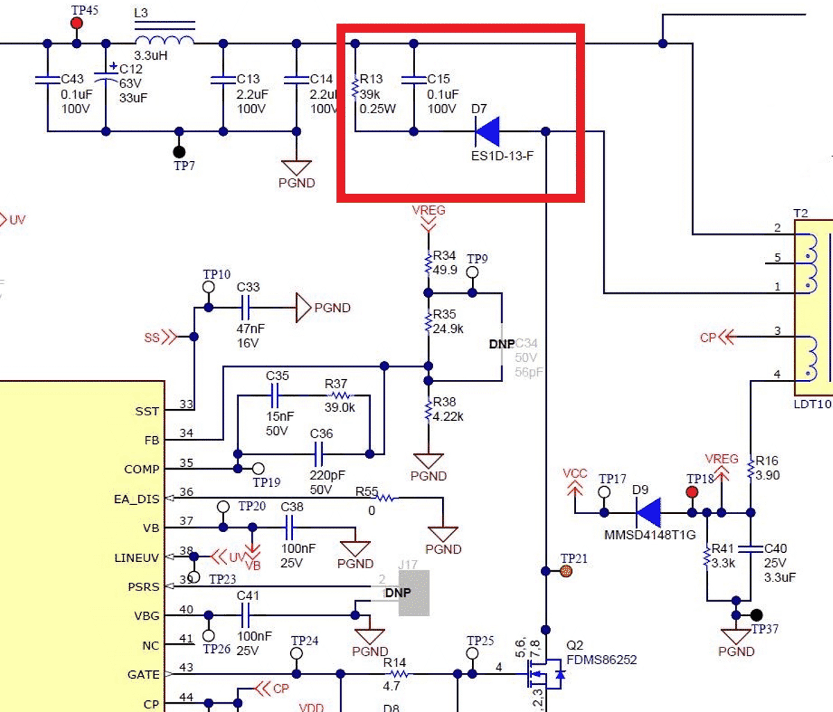 Figure 3-12 Primary MOSFET RCD Clamp
If it is primary side regulation (PSR), the feedback loop is on the primary side. These components should be close to what we use in our reference designs. The transformer design is a critical part of the functionality of PSR. Since the transformer sets the primary currents, plays an important role in the regulation of the primary loop and sets the auxiliary voltage level, the entire primary side (and secondary side) would need to be redesigned.
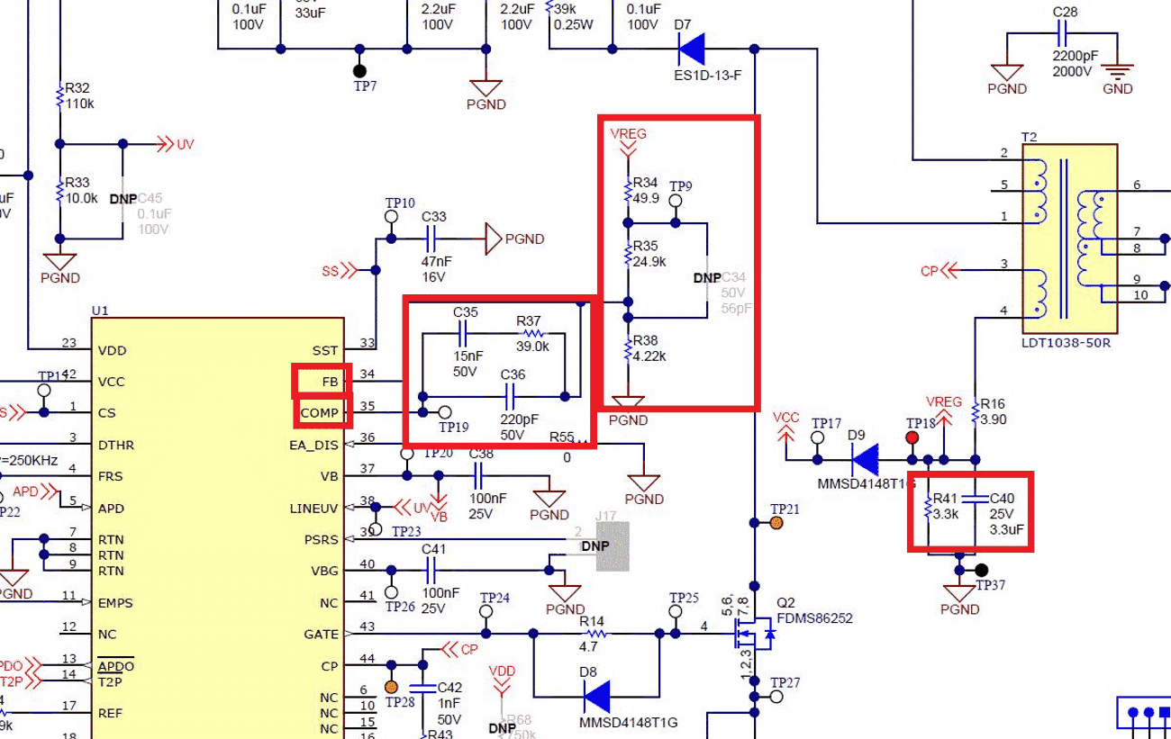 Figure 3-13 Primary Side Regulation (PSR) Feedback Components
The Transformer: This is the most critical component of the DCDC. It sets everything else. The best thing for to do is to use the exact transformer used in the EVM/reference design. Otherwise, much of the design will need to be re-calculated. For flybacks, for active clamp forwards. For non-PSR transformers, the transformer can be swapped out, but check: the primary inductance, the turns ratios, the DCR, leakage inductance, transformer size/footprint, the switching frequency, and power rating. If these are changed, then other parts of the design will need to reviewed. PSR regulation is highly dependent on the way the transformer layers are stacked and wound. The winding has to be spread across the entire bobbin. The stackup should have the auxiliary between the secondary windings, and the primary should be split. These are typically not shown in the spec sheet, it is recommended using transformers in TI EVMs and reference designs. The stackup are as follows:
- ½ pri
- Gate drive
- Secondary
- Bias/aux
- ½ pri
Ensure there are common mode capacitors – they help with EMI and TI recommends them.
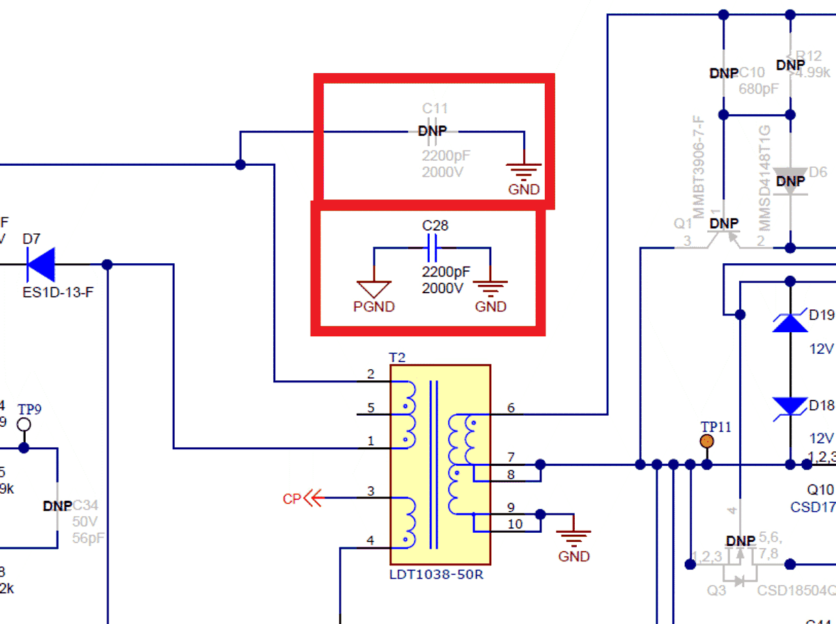 Figure 3-14 Common Mode Capacitors