SLVAF88 September 2021 LM74720-Q1 , LM74721-Q1 , LM74722-Q1
1 Application Brief
Introduction
In systems powered by internal combustion engines, alternator provides power to the automotive electrical system by charging the battery during normal runtime of the vehicle. Rectified alternator output voltage can contain AC voltage ripple superimposed on the battery voltage during entire life time of the vehicle depending on the operating conditions. The AC voltage ripple is superimposed on the DC battery line due to variation in engine speed, regulator duty cycle with field current switching ON/OFF and electrical load variations. In fully electric systems or semi-hybrid systems, the entire electrical load is fed through DC-DC converters. In the absence power supply line choke, the output voltage of DC-DC converter can inject AC voltage ripple superimposed on the DC output voltage.
The reverse battery protection circuit is typically the first sub-system which is present at the input of Automotive ECUs. Hence the reverse battery protection circuit is verified for uninterrupted and stable operation with AC voltage ripple superimposed on the battery supply line by testing its reverse battery protection circuit according to different automotive test standards.
Automotive Standards on AC Superimposed Tests
AC superimposed tests are specified in various automotive test standards such as ISO 16750-2, LV124 and other OEM specific standards and are intended to verify stable operation of various electronic modules. Standards such as ISO 16750-2 specifies AC ripple of 2-V Peak-Peak on a 13.5-V DC battery voltage, swept from 50 Hz to 25 kHz and the test waveform is shown in Figure 1-1. Other manufacturer specific requirements such as VW 80000, TS-0000425-05 can vary and the frequency can go up to 200 kHz. Peak-Peak ripple amplitude varies from 1-V peak-peak to 6-V peak-peak, depending on the location of module with reference to Alternator, DC-DC converter and Battery.
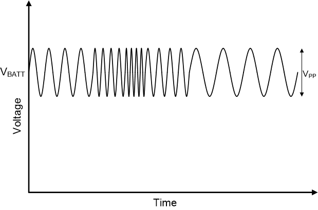 Figure 1-1 AC Super Imposed Test
Why it is necessary to rectify AC voltage ripple
Conventional input protection circuits use either a Schottky diode or a P-Channel MOSFET based circuit to provide reverse battery protection. Schottky diode rectifies the AC ripple superimposed on the battery voltage effectively. The challenge with Schottky diode is the high power dissipation due to high forward voltage drop across it. Schottky diode is suitable to be used only in very low power designs.
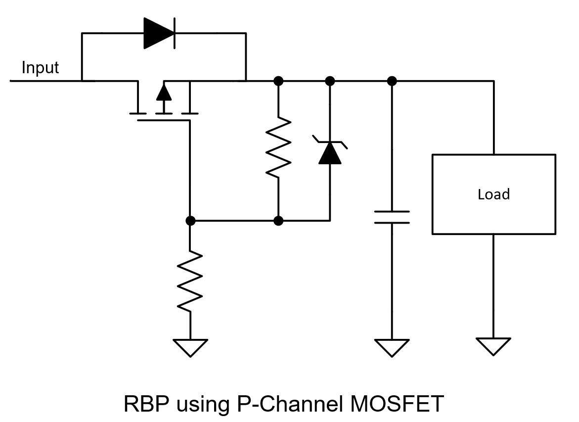
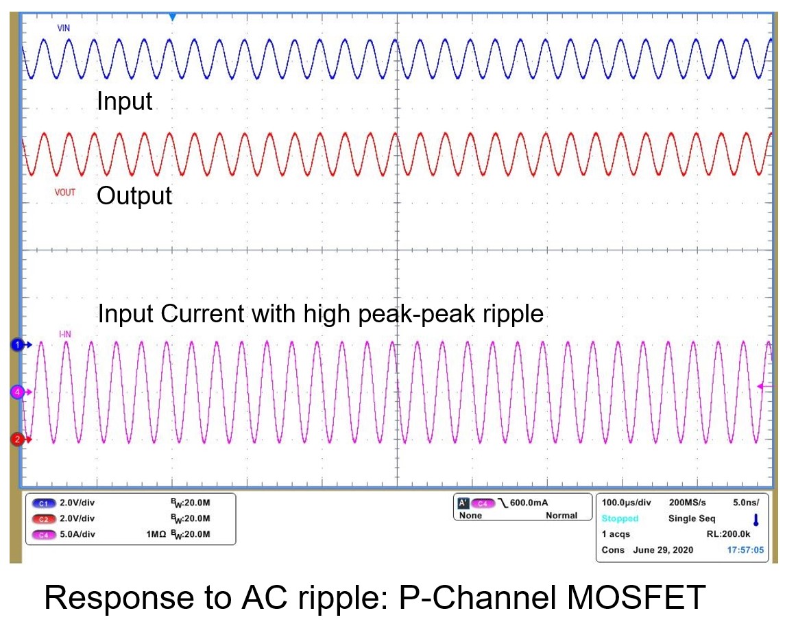 Figure 1-2 Reverse
Battery Protection:
 P-Channel MOSFET
Also, reverse battery protection circuit shown in Figure 1-2 using a P-Channel MOSFET does not block reverse current and hence the AC ripple voltage is not rectified. Since AC ripple is not rectified, output voltage follows input voltage and the AC ripple current swings negative leading to increase in peak-peak ripple current and RMS ripple current.
The RMS ripple current flows through the output electrolytic capacitors and causes power dissipation in them. The power dissipation in the output capacitors increase as the ripple current magnitude increases. This ripple current if not limited can increase the aging effect and reduce overall reliability. Rectification of the AC voltage ripple superimposed on DC voltage is necessary for applications such as Sensor Fusion which can have capacitance in the order of few milli-Farads to solve these problems. Rectification of the ripple at the input also helps improve the PSRR of the supply which is beneficial for Audio Amplifier sub-system.
Active Rectification using LM7472x-Q1 Family of Ideal Diode Controllers
The LM7472x-Q1 family of ideal diode controller features a dual-gate drives topology to control two external back to back N-Channel MOSFETs. One of the MOSFET is controlled to emulate an ideal diode and another MOSFET for power path ON/OFF control, inrush current limiting and over voltage protection.
Ideal Diode Controller LM7472x-Q1 family of devices features a very low forward drop (13 mV) to minimize power dissipation in the N-Channel MOSFET during normal operation. LM7472x-Q1 integrates a boost converter to provide voltage necessary to drive the external N-channel MOSFETs for the ideal diode and the load disconnect stages.
LM7472x-Q1 rectifies the AC superimposed voltage by turning the MOSFET Q1 OFF quickly to cut off reverse current and turning the MOSFET Q1 ON quickly during forward conduction. A simplified schematic showing ideal diode used for active rectification is shown in Figure 1-3. For complete application circuit, refer to the LM74720-Q1 and LM74722-Q1 data sheet application section.
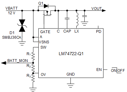 Figure 1-3 LM74722-Q1 in Ideal Diode Only Configuration
The integrated boost regulator has a high loading capacity of 30 mA. The high peak GATE drive current of LM7472x-Q1 family of devices along with short turn ON and turn OFF delay times of comparators result in fast Turn ON and Turn OFF of the N-channel MOSFET for the ideal diode. The LM74720-Q1 and LM74721-Q1 can drive the gate-source voltage of the MOSFET within 1.9 µs (typical). Higher peak gate drive strength of LM74722-Q1 enables even faster turn ON of the GATE. LM74722-Q1 can drive the gate-source voltage of the MOSFET within 0.8 µs (typical). LM7472x-Q1 also offer very fast turn OFF delay. These very short switching times allow LM74720-Q1 and LM74721-Q1 to be used for rectification of 100 kHz AC voltage ripple where as LM74720-Q1 can rectify 200 kHz AC ripple.
Active rectification of 2-V peak-peak, 200 kHz AC voltage ripple by LM74722-Q1 is captured in Figure 1-4. During the positive cycle MOSFET is turned ON, output capacitor charges and output follows input until the current through the MOSFET reverses. As soon as reverse current is detected, LM7472x-Q1 turns OFF the MOSFET within 0.45 µs, thereby blocking the reverse current completely. In the negative cycle, output capacitor discharges at a constant rate determined by the load current and amount of output capacitance.
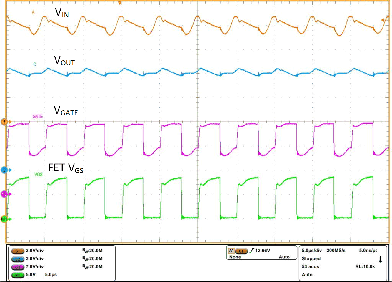 Figure 1-4 AC Super Imposed Test – 2-V Peak-Peak 200 kHz
Fast reverse current blocking minimizes the peak reverse current and completely block reverse current during the negative cycle. Thus AC ripple current RMS value is reduced by half which in-turn reduces the power dissipation in the output electrolytic capacitor ESR by half.
Very low forward voltage drop and reduced RMS ripple current reduces the power dissipation in the MOSFET as well.
Summary
Efficient active rectification of AC ripple superimposed on DC voltage results in low forward voltage drop, reduced RMS ripple current leading to lower power dissipation in MOSFET and output electrolytic capacitors and improved PSRR. Hence, Ideal diodes which perform active rectification become an inevitable choice for designing reverse battery protection subsystem in automotive ECU designs. Key performance features such as very low forward voltage drop, fast gate drive, fast reverse recovery response and integrated boost converter enables LM7472x-Q1 family of ideal diode controllers to achieve active rectification of AC voltage ripple with frequencies up to 200 kHz.