SLVAF89 November 2021 TLV61046A , TLV61048 , TPS61040 , TPS61041 , TPS61045 , TPS61046 , TPS61085 , TPS61086 , TPS61088 , TPS61089 , TPS61096A , TPS61170 , TPS61175 , TPS61178 , TPS61288
1 Introduction
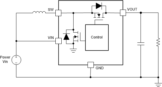
Many applications require a boost converter to obtain an output voltage higher than the input voltage. For boost converters, the VIN pin is connected to the power supply of the device, while the SW pin is connected to the drain of the internal low-side power MOSFET. Figure 1-1 shows the typical application of a boost converter. The power supply Vin of power stage is used as the source of the VIN pin so Vin should be compatible with the input voltage range of the device.
 Figure 1-1 Typical Application of Synchronous Boost
Converter
Figure 1-1 Typical Application of Synchronous Boost
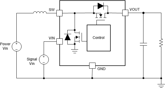
ConverterHowever, boost converters have strict restrictions on the input voltage range. It is not easy to choose an appropriate boost converter in some applications, especially when the power stage needs to work with very low input voltage. Figure 1-2 shows a simple solution using an external bias signal Vin for the VIN pin. The Vin signal should be compatible with the input voltage range but it is only for the IC itself, so the current consumption is only at the mA level. The actual power supply for boost power stage power Vin can be much wider than the input voltage range.
 Figure 1-2 External Bias Application of Synchronous
Boost Converter