SLVAF89 November 2021 TLV61046A , TLV61048 , TPS61040 , TPS61041 , TPS61045 , TPS61046 , TPS61085 , TPS61086 , TPS61088 , TPS61089 , TPS61096A , TPS61170 , TPS61175 , TPS61178 , TPS61288
3 Applicable Devices List and Test Results
According to the previously-analyzed requirements, the middle-voltage boost converters that support external bias are listed and divided based on their control strategies in Table 3-1.
| Main Control Strategy | Control Strategy at Light Load | Devices Supporting External Bias |
|---|---|---|
| Fixed Frequency Modulation | Pulse Skipping Mode | TPS61175(1), TPS61170 |
| Pulse Frequency Modulation | TPS61178(2) | |
| Forced PWM Mode | TPS61175(1), TPS611781(2), TPS61080, TPS61081 | |
| Quasi-Constant Frequency Modulation | Pulse Skipping Mode | TPS61086, TPS61046, TLV61046a, TLV61048, TPS61085 |
| Pulse Frequency Modulation | TPS61288, TPS61088, TPS61089 | |
| Forced PWM Mode | TPS610891 | |
| Pulse Frequency Modulation | Pulse Frequency Modulation | TPS61045, TPS61040, TPS61041, TPS61096a |
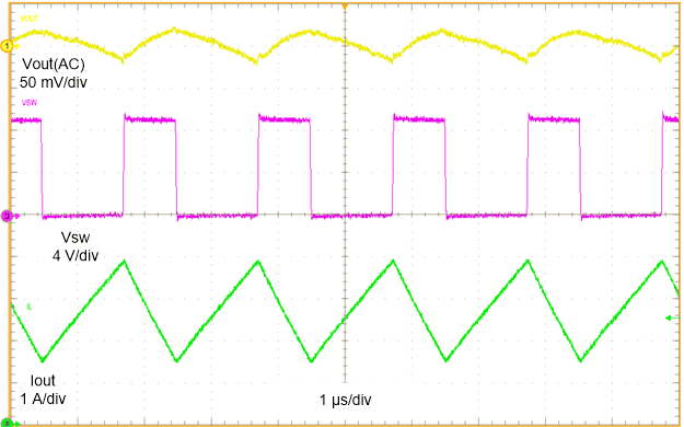
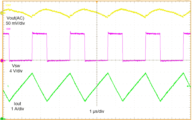
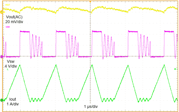
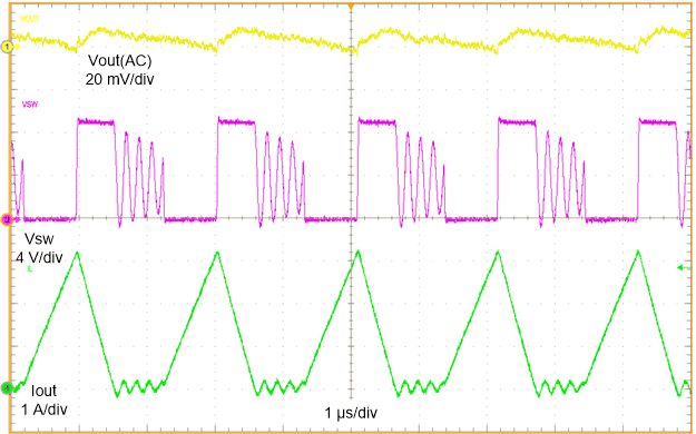
Take the TPS61089 as an example. Figure 3-1, Figure 3-2, Figure 3-3, and Figure 3-4 show the main waveforms with external bias and without external bias in CCM and DCM, respectively. When power Vin equals to signal Vin, there is no difference for the device so the waveforms are the same. This assures that the TPS61089 can be used in external bias applications.
With external bias, the input voltage range of the TPS61089 can be extended as previously analyzed. Figure 3-5 shows the waveforms of the TPS61089 when the signal Vin is 3.6 V while the power Vin is only 1.5 V. Compared with the 2.7-V minimum input voltage for a typical application, the device can work with much lower input voltage as long as the current limit is not reached.
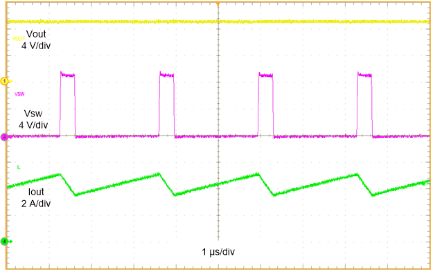 Figure 3-5 TPS61089 Power Vin = 1.5 V, Signal Vin
= 3.6 V, Vo = 9 V, Io = 1 A