SLVAFB4 July 2022 TPS62902-Q1 , TPS62903 , TPS62903-Q1
4 Typical Performance and Waveforms
The application circuit shown in Figure 4-1 is used to generate the data for typical performance. There is no reference design for the TPS6290x using inverting buck-boost topology. The buck EVM was modified to be used as an inverting buck-boost. See How to Modify a Step-Down Converter to Inverting Buck-Boost Topology for details. L1 is a 1µH inductor XGL4020-102MEC from Coilcraft. The output capacitors used 3x22 µF, 10 V, 0805, X7S ceramic capacitor. The input capacitor used 10 μF, 25V, 1206, X7R. Unless otherwise specified, VIN = 12 V and VOUT = –3.3 V, IOUT=0 A to 2.1A, 2.5 MHz, Auto PFM/PWM, internal feedback (VSET).
 Figure 4-1 Schematic
of Tested Circuit
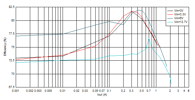 Figure 4-2
Efficiency with VOUT = –3.3 V
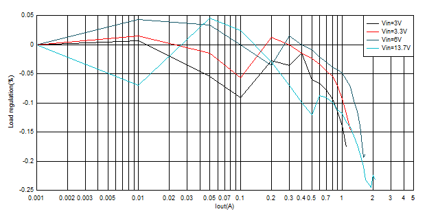 Figure 4-3 Load
Regulation with VOUT = –3.3 V
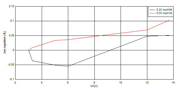 Figure 4-4 Line
Regulation with VOUT = –3.3 V , IOUT = 0 A and 1A
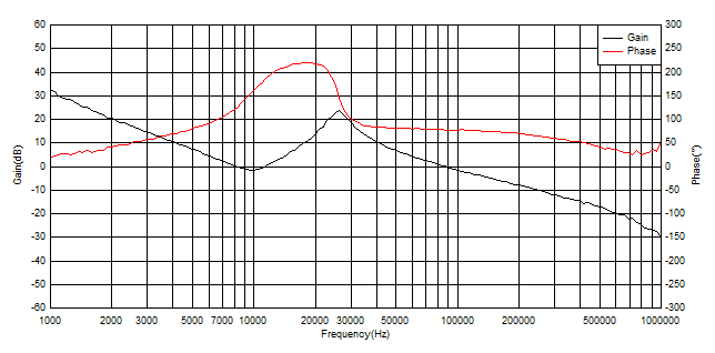 Figure 4-5 Loop
Response with VIN =12 V, VOUT = –3.3 V, IOUT =
2A
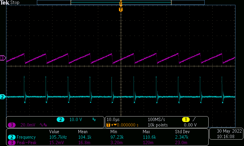 Figure 4-6 Output
Voltage Ripple with VIN = 12 V, VOUT = -3.3 V,
IOUT = 30mA
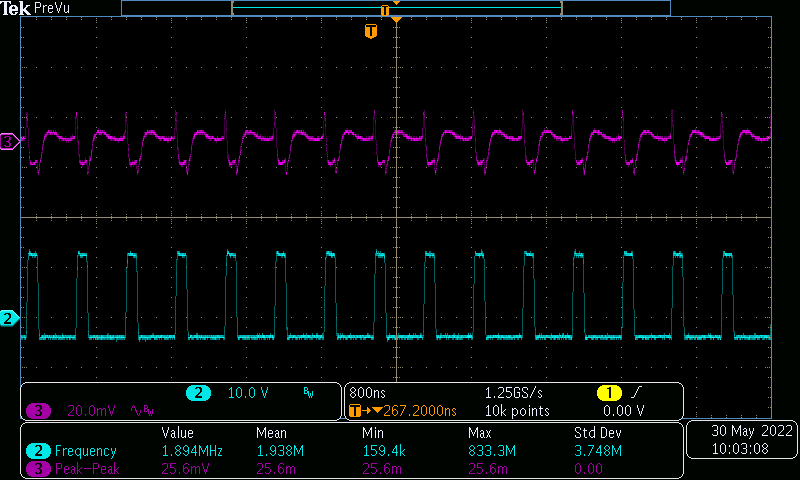 Figure 4-7 Output
Voltage Ripple with VIN = 12 V, VOUT = -3.3 V,
IOUT = 2A
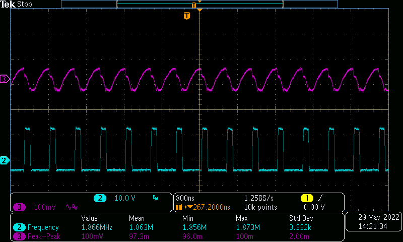 Figure 4-8 Input
Voltage Ripple with VIN = 12 V , VOUT = -3.3 V,
IOUT = 2A
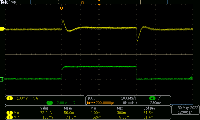 Figure 4-9 Load Transient with
VIN = 12 V, VOUT = -3.3 V, IOUT = 0.1 A to
2A
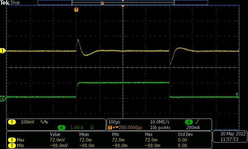 Figure 4-10 Load Transient with
VIN = 3.3V, VOUT = -3.3 V, IOUT = 0.1 A to
1A