SLVAFB4 July 2022 TPS62902-Q1 , TPS62903 , TPS62903-Q1
2.3 Power Good Pin
The TPS62903 has a built-in power good (PG) function to indicate whether the output voltage has reached its appropriate level or not. The PG pin is an open-drain output that requires a pullup resistor. Because - VOUT is the IC ground in this configuration, the PG pin is referenced to -VOUT instead of ground, which means that the TPS62903 pulls PG to -VOUT when it is low.
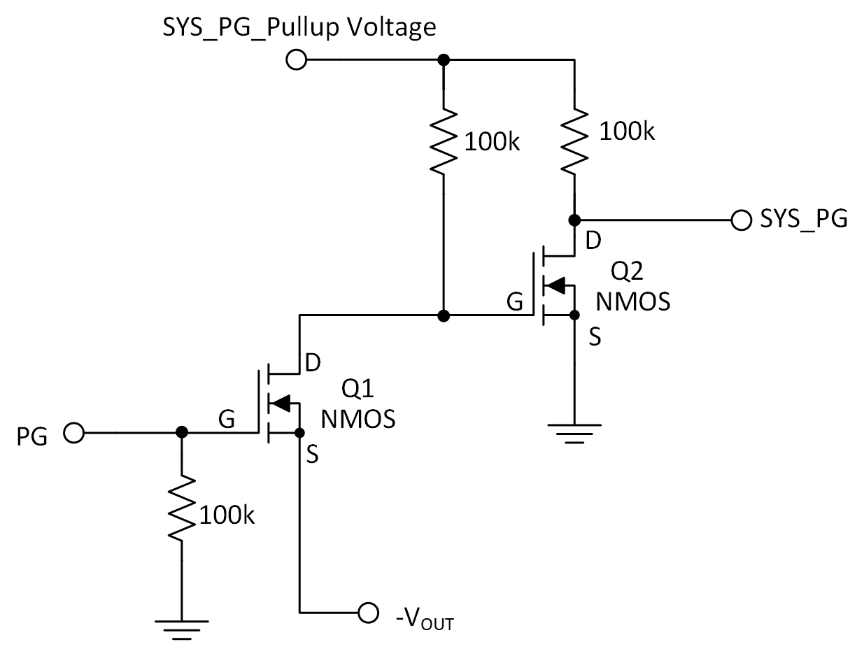
This behavior can cause difficulties in reading the state of the PG pin, because in some applications the IC detecting the polarity of the PG pin might not be able to withstand negative voltages. The level shifter circuit shown in Figure 2-4 alleviates any difficulties associated with the offset PG pin voltages by eliminating the negative output signals of the PG pin. If the PG pin functionality is not needed, it can be left floating without this circuit. Note that to avoid violating its absolute maximum rating, the PG pin should not be driven more than 17 V above the negative output voltage (IC ground).
 Figure 2-4 PG Pin Level Shifter
Connecting TPS62903 PG pin to the gate of Q1, when the PG pin is pulled low(-VOUT), Q1 is off and Q2 is on because its VGS sees SYS_PG_Pullup Voltage. SYS_PG is then pulled to ground.
When PG pin is pulled high(GND), the gate of Q1 is pulled to ground potential turning it on. This pulls the gate of Q2 below ground, turning it off. SYS_PG is then pulled up to its pullup voltage. Note that the pullup voltage must be at an appropriate logic level for the circuitry connected to the SYS_PG. A small size dual N Channel 20V(D-S) MOSFET Si1902CDL from Vishay can be used in the design.