SLVAFE7 September 2022 LM51551
2.2 Switching Frequency Shift
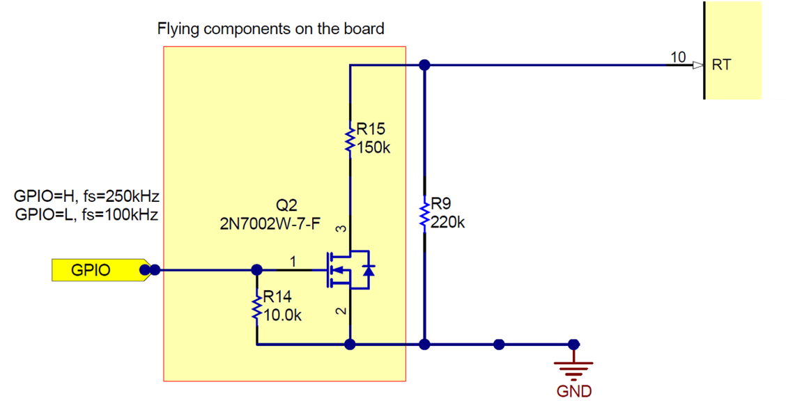
As previously mentioned, the switching frequency for SMPS is set by the resistor. The frequency stays constant during all the transmitting period which forces the MOSFET working at a high frequency. That leads to the high-quiescent dissipation of the control chip. In this application note, a MOSFET combined with two additional resistors are used to change the switching frequency at the no-load period. The signal from GPIO can set the Fsw from 250 kHz to 100 kHz, which is only 46 mW at the maximum output voltage.
 Figure 2-3 Switching Frequency Control by GPIO