SLVAFE7 September   2022 LM51551


  1.   Abstract
  2.   Trademarks
  3. 1Introduction
    1. 1.1 Design Specification and Key Challenges
  4. 2High-Voltage Power Supply Design Using SEPIC
    1. 2.1 TI HV Supply Architecture Using SEPIC Topology
    2. 2.2 Switching Frequency Shift
    3. 2.3 Voltage Control by External Signal
  5. 3Test Result
    1. 3.1 Efficiency and Power Consumption (100 kHz vs 250 kHz)
    2. 3.2 Linearity of Output Voltages vs VBIAS
    3. 3.3 Output Ripple Measurement
    4. 3.4 Load Transient Test
    5. 3.5 Overload Protection
    6. 3.6 Thermal Image
  6. 4Summary
  7. 5References

Thermal Image

Figure 3-15 shows the thermal image of the high-voltage power supply board after testing for 20 minutes. With the 12-V input, ±75 V/1.5 W output operation, the maximum temperature is 42.7°C in the top side at an ambient temperature of 22°C.
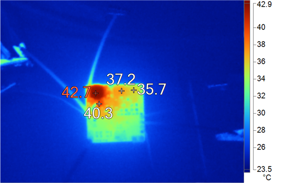
GUID-20220808-SS0I-XTQN-22W0-9WZ2P3KWNT2C-low.png Figure 3-15 Thermal Performance of the Design