SLVAFN4 October 2023 TCA9509 , TCA9517A
2 Contrasting Setups of SVO Buffers
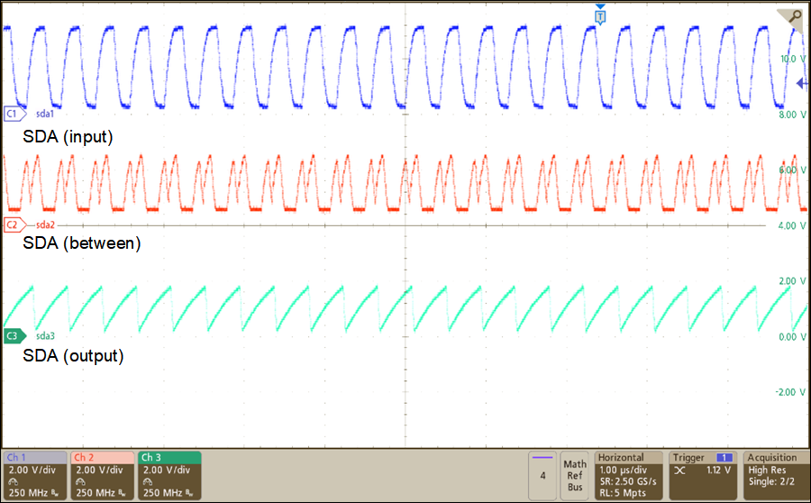
As seen in Figure 2-1, the two sides containing the SVO are connected together, which must not be carried out. Note that the SVO output voltage output low (VOL) is considered to be “buffered low”, which is generally higher than the VOL levels of other peripheral devices. Similarly, the voltage output low of the external device (VOL,EXT) is required to be less than the voltage input low contention (VILC) at the SVO side to be able to be propagated as an input low into the buffer. These characteristics of the SVO feature result in a gap between the buffered VOL of the first device and the VILC requirement of the second device. In other words, the VOL of 0.52 V is higher than the VILC of 0.4 V, so an input low of the first buffer is unable to propagate a low to the second buffer correctly. For more information regarding the SVO feature, see also the Why, When, and How to use I2C Buffers application note.
 Figure 2-1 Schematic of
Improper Implementation of Two TCA9517s
 Figure 2-2 Waveforms as
a Result of Improper Setup (Address 0x70h Sent)
Figure 2-2 Waveforms as
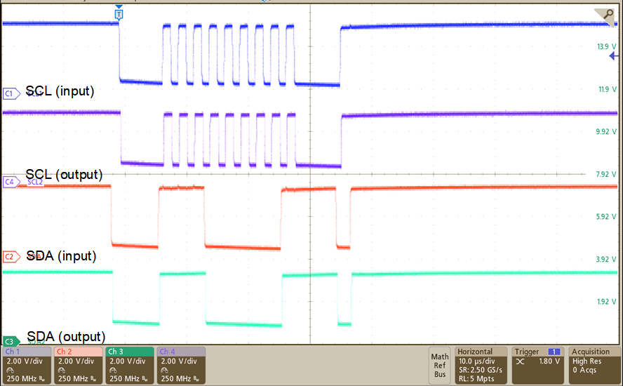
a Result of Improper Setup (Address 0x70h Sent)To resolve the implementation issue, the TCA9509 can be used in place of the second TCA9517 as shown in Figure 2-3, allowing for both the B side of the devices to be connected together. This device has the SVO on the A side instead of the B side, which mitigates the concern of improper SVO sides being connected together. The improved performance is shown in Figure 2-4.
 Figure 2-3 Schematic of
Proper Implementation of Buffers With SVO
  Figure 2-4 Waveforms as
a Result of Proper Setup (Address 0x70h Sent)