SLVS203F
June 1999 – January 2025
TPS769
PRODUCTION DATA
1
1
Features
2
Applications
3
Description
4
Pin Configuration and Functions
5
Specifications
5.1
Absolute Maximum Ratings
5.2
ESD Ratings
5.3
Recommended Operating Conditions
5.4
Thermal Information (New Chip)
5.5
Thermal Information (Legacy Chip)
5.6
Electrical Characteristics
5.7
Typical Characteristics
5.8
Typical Characteristics: Supported ESR Range
6
Detailed Description
6.1
Overview
6.2
Functional Block Diagrams
6.3
Feature Description
6.3.1
Output Enable
6.3.2
Dropout Voltage
6.3.3
Current Limit
6.3.4
Undervoltage Lockout (UVLO)
6.3.5
Output Pulldown
6.3.6
Thermal Shutdown
6.4
Device Functional Modes
6.4.1
Normal Operation
6.4.2
Dropout Operation
6.4.3
Disabled
7
Application and Implementation
7.1
Application Information
7.2
Typical Application
7.2.1
Design Requirements
7.2.2
Detailed Design Procedure
7.2.2.1
Adjustable Device Feedback Resistors
7.2.2.2
Recommended Capacitor Types
7.2.2.3
Input and Output Capacitor Requirements
7.2.2.4
Reverse Current
7.2.2.5
Feed-Forward Capacitor (CFF)
7.2.2.6
Power Dissipation (PD)
7.2.2.7
Estimating Junction Temperature
7.2.3
Application Curves
7.3
Power Supply Recommendations
7.4
Layout
7.4.1
Layout Guidelines
7.4.2
Layout Example
8
Device and Documentation Support
8.1
Device Support
8.1.1
Development Support
8.1.1.1
Evaluation Module
8.1.1.2
Spice Models
8.1.1.3
Device Nomenclature
8.2
Documentation Support
8.2.1
Related Documentation
8.3
Receiving Notification of Documentation Updates
8.4
Support Resources
8.5
Trademarks
8.6
Electrostatic Discharge Caution
8.7
Glossary
9
Revision History
10
Mechanical, Packaging, and Orderable Information
5.7
Typical Characteristics
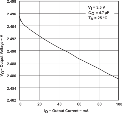
Figure 5-1
TPS76925 Output Voltage vs Output Current
(Legacy Chip)
Figure 5-3
TPS76933 Output Voltage vs Output Current
(Legacy Chip)
T
J
= 25°C
Figure 5-5
TPS76933 Output Voltage vs Output Current
(New Chip)
Figure 5-2
TPS76915 Output Voltage vs Output Current
(Legacy Chip)
T
J
= 25°C
Figure 5-4
TPS76933 Output Voltage vs Output Current
(New Chip)
Figure 5-6
TPS76915 Output Voltage vs Free-Air Temperature (Legacy Chip)
Figure 5-7
TPS76925 Output Voltage vs Free-Air Temperature (Legacy Chip)
Figure 5-9
TPS76933 Output Voltage vs Free-Air Temperature (New Chip)
Figure 5-11
TPS76933 Load Regulation vs Free-Air Temperature (New Chip)
Figure 5-13
TPS76933 Ground Current vs Free-Air Temperature (New Chip)
Figure 5-15
TPS76933 Ground Current vs Output Current
(New Chip)
Figure 5-17
TPS76933 Ground Current vs Input Supply
(New Chip)
Figure 5-19
TPS76933 EN Threshold vs Free-Air Temperature (New Chip)
Figure 5-21
TPS76933 Output Spectral Noise Density vs Frequency (Legacy Chip)
Figure 5-23
TPS76933 Output Spectral Noise Density vs Output Capacitor (New Chip)
Figure 5-25
Output Impedance vs Frequency (Legacy Chip)
Figure 5-27
TPS76933 Dropout Voltage vs Free-Air Temperature (New Chip)
Figure 5-29
TPS76901 Dropout Voltage vs Input Supply
(New Chip)
Figure 5-31
TPS76933 Ripple Rejection vs Output Current
(New Chip)
I
OUT
= 50mA
Figure 5-33
TPS76901 Ripple Rejection vs Feed-Forward Capacitor (New Chip)
Figure 5-35
LDO Start-Up Time With Input Supply (New Chip)
Figure 5-37
TPS76915 Line Transient Response (Legacy Chip)
Figure 5-39
TPS76933 Line Transient Response (Legacy Chip)
4.3V to 16.0V at 1V/μs
Figure 5-41
TPS76933 Line Transient Response (New Chip)
1mA to 100mA at 1A/μs
Figure 5-43
TPS76933 Load Transient Response (New Chip)
1mA to 100mA at 1mA/μs
Figure 5-45
TPS76933 Load Transient Response (New Chip)
Figure 5-8
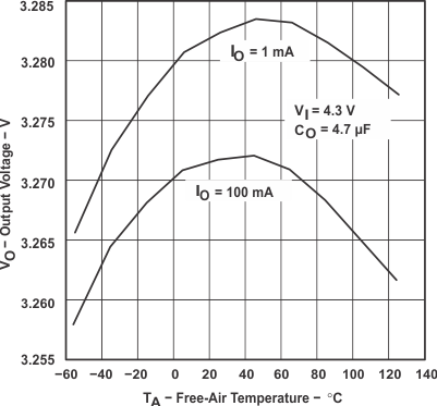
TPS76933 Output Voltage vs Free-Air Temperature (Legacy Chip)
Figure 5-10
TPS76933 Line Regulation vs Free-Air Temperature (New Chip)
Figure 5-12
TPS76933 Ground Current vs Free-Air Temperature (Legacy Chip)
T
J
= 25°C
Figure 5-14
TPS76933 Ground Current vs Output Current
(New Chip)
Figure 5-16
TPS76933 Ground Current vs Input Supply
(New Chip)
Figure 5-18
TPS76933 UVLO Threshold vs Free-Air Temperature (New Chip)
Figure 5-20
TPS76933 Current Limit vs Free-Air Temperature (New Chip)
Figure 5-22
TPS76933 Output Spectral Noise Density vs Output Current (New Chip)
I
OUT
= 50mA
Figure 5-24
TPS76901 Output Spectral Noise Density vs Feed-Forward Capacitor (New Chip)
Figure 5-26
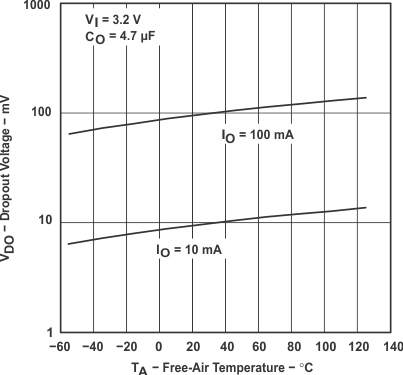
TPS76933 Dropout Voltage vs Free-Air Temperature (Legacy Chip)
Figure 5-28
TPS76933 Dropout Voltage vs Output Current
(New Chip)
Figure 5-30
TPS76933 Ripple Rejection vs Frequency
(Legacy Chip)
I
OUT
= 100mA
Figure 5-32
TPS76933 Ripple Rejection vs Output Capacitor (New Chip)
Figure 5-34
LDO Start-Up Time (Legacy Chip)
Figure 5-36
LDO Start-Up Time With EN (New Chip)
Figure 5-38
TPS76915 Load Transient Response (Legacy Chip)
4.3V to 5.3V at 1V/μs
Figure 5-40
TPS76933 Line Transient Response (New Chip)
Figure 5-42
TPS76933 Load Transient Response (Legacy Chip)
1μA to 100mA at 1A/μs
Figure 5-44
TPS76933 Load Transient Response (New Chip)