SLVS876D November 2008 – November 2014 TPS54232
PRODUCTION DATA.
- 1 Features
- 2 Applications
- 3 Description
- 4 Simplified Schematic
- 5 Revision History
- 6 Pin Configuration and Functions
- 7 Specifications
-
8 Detailed Description
- 8.1 Overview
- 8.2 Functional Block Diagram
- 8.3
Feature Description
- 8.3.1 Fixed-Frequency PWM Control
- 8.3.2 Voltage Reference (Vref)
- 8.3.3 Bootstrap Voltage (BOOT)
- 8.3.4 Enable and Adjustable Input Undervoltage Lockout (VIN UVLO)
- 8.3.5 Programmable Slow-Start Using SS Pin
- 8.3.6 Error Amplifier
- 8.3.7 Slope Compensation
- 8.3.8 Current Mode Compensation Design
- 8.3.9 Overcurrent Protection and Frequency Shift
- 8.3.10 Overvoltage Transient Protection
- 8.3.11 Thermal Shutdown
- 8.4 Device Functional Modes
-
9 Application and Implementation
- 9.1 Application Information
- 9.2
Typical Application
- 9.2.1 Design Requirements
- 9.2.2 Detailed Design Procedure
- 9.2.3 Application Curves
- 10Power Supply Recommendations
- 11Layout
- 12Device And Documentation Support
- 13Mechanical, Packaging, And Orderable Information
9 Application and Implementation
NOTE
Information in the following applications sections is not part of the TI component specification, and TI does not warrant its accuracy or completeness. TI’s customers are responsible for determining suitability of components for their purposes. Customers should validate and test their design implementation to confirm system functionality.
9.1 Application Information
The TPS54232 device is typically used as a step-down converter, which converts a voltage from 3.5 V to 28 V to a lower voltage. WEBENCH™ software is available to aid in the design and analysis of circuits.
For additional design needs, see:
| TPS54231 | TPS54232 | TPS54233 | TPS54331 | TPS54332 | |
|---|---|---|---|---|---|
| IO(Max) | 2A | 2A | 2A | 3A | 3.5A |
| Input Voltage Range | 3.5V - 28V | 3.5V - 28V | 3.5V - 28V | 3.5V - 28V | 3.5V - 28V |
| Switching Freq. (Typ) | 570kHz | 1000kHz | 285kHz | 570kHz | 1000kHz |
| Swiitch Current Limit (Min) | 2.3A | 2.3A | 2.3A | 3.5A | 4.2A |
| Pin/Package | 8SOIC | 8SOIC | 8SOIC | 8SOIC | 8SO PowerPAD™ |
9.2 Typical Application
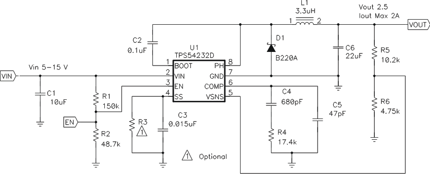 Figure 10. Typical Application Schematic
9.2.1 Design Requirements
For this design example, use the values listed in Table 2 as the input parameters
Table 2. Design Parameters
| DESIGN PARAMETER | EXAMPLE VALUE |
|---|---|
| Input voltage range | 5 V to 15V |
| Output voltage | 2.5 V |
| Input ripple voltage | 300 mV |
| Output ripple voltage | 30 mV |
| Output current rating | 2 A |
| Operating Frequency | 1 MHz |
9.2.2 Detailed Design Procedure
The following design procedure can be used to select component values for the TPS54232. Alternately, the WEBENCH Software may be used to generate a complete design. The WEBENCH™ Software uses an iterative design procedure and accesses a comprehensive database of components when generating a design. This section presents a simplified discussion of the design process.
9.2.2.1 Switching Frequency
The switching frequency for the TPS54232 is fixed at 1 MHz.
9.2.2.2 Output Voltage Set Point
The output voltage of the TPS54232 is externally adjustable using a resistor divider network. In the application circuit of Figure 10, this divider network is comprised of R5 and R6. The relationship of the output voltage to the resistor divider is given by Equation 4 and Equation 5.
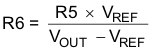
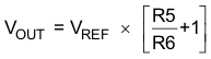
Choose R5 to be approximately 10 kΩ. Slightly increasing or decreasing R5 can result in closer output voltage matching when using standard value resistors. In this design, R4 = 10.2 kΩ and R = 4.75 kΩ, resulting in a 2.5 V output voltage. The zero ohm resistor R4 is provided as a convenient place to break the control loop for stability testing.
9.2.2.3 Input Capacitors
The TPS54232 requires an input decoupling capacitor and depending on the application, a bulk input capacitor. The typical recommended value for the decoupling capacitor is 10 μF. A high-quality ceramic type X5R or X7R is recommended. The voltage rating should be greater than the maximum input voltage. A smaller value may be used as long as all other requirements are met; however 10 μF has been shown to work well in a wide variety of circuits. Additionally, some bulk capacitance may be needed, especially if the TPS54232 circuit is not located within about 2 inches from the input voltage source. The value for this capacitor is not critical but should be rated to handle the maximum input voltage including ripple voltage, and should filter the output so that input ripple voltage is acceptable. For this design a 10 μF capacitor issued for the input decoupling capacitor. It isX5R dielectric rated for 25 V. The equivalent series resistance (ESR) is approximately 5 mΩ, and the current rating is 3 A.
This input ripple voltage can be approximated by Equation 6.
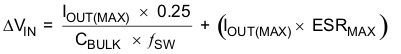
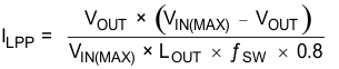
Where IOUT(MAX) is the maximum load current, fSW is the switching frequency, CBULK is the input capacitor value and ESRMAX is the maximum series resistance of the input capacitor.
The maximum RMS ripple current also needs to be checked. For worst case conditions, this can be approximated by Equation 7.
In this case, the input ripple voltage would be 60 mV and the RMS ripple current would be 1 A. It is also important to note that the actual input voltage ripple will be greatly affected by parasitics associated with the layout and the output impedance of the voltage source. The actual input voltage ripple for this circuit is shown in Table 2 and is larger than the calculated value. This measured value is still below the specified input limit of 300 mV. The maximum voltage across the input capacitors would be VIN max plus ΔVIN/2. The chosen bulk and bypass capacitors are each rated for 25 V and the ripple current capacity is greater than 3 A, both providing ample margin. It is very important that the maximum ratings for voltage and current are not exceeded under any circumstance.
9.2.2.4 Output Filter Components
Two components need to be selected for the output filter, L1 and C3. Since the TPS54232 is an externally compensated device, a wide range of filter component types and values can be supported.
9.2.2.4.1 Inductor Selection
To calculate the minimum value of the output inductor, use Equation 8.
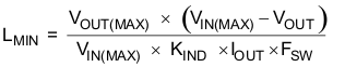
KIND is a coefficient that represents the amount of inductor ripple current relative to the maximum output current. In general, this value is at the discretion of the designer; however, the following guidelines may be used. For designs using low ESR output capacitors such as ceramics, a value as high as KIND = 0.4 may be used. When using higher ESR output capacitors, KIND = 0.2 yields better results.
For this design example, use KIND = 0.35 and the minimum inductor value is calculated to be 2.97 μH. For this design, a large value was chosen: 3.3 μH.
For the output filter inductor, it is important that the RMS current and saturation current ratings not be exceeded. The peak-to-peak inductor current is calculated using Equation 9.
The RMS inductor current can be found from Equation 10.
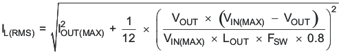
and the peak inductor current can be determined with Equation 11.
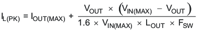
For this design, the RMS inductor current is 2.01 A and the peak inductor current is 2.39 A. The chosen inductor is a Coilcraft MSS7341-332NL 3.3 μH. It has a saturation current rating of 3.28 A and an RMS current rating of 3.95 A, meeting these requirements. Smaller or larger inductor values can be used depending on the amount of ripple current the designer wishes to allow so long as the other design requirements are met. Larger value inductors will have lower ac current and result in lower output voltage ripple, while smaller inductor values will increase ac current and output voltage ripple. Inductor values for use with the TPS54232 are in the range of 1 μH to 47 μH.
9.2.2.4.2 Capacitor Selection
The important design factors for the output capacitor are dc voltage rating, ripple current rating, and equivalent series resistance (ESR). The dc voltage and ripple current ratings cannot be exceeded. The ESR is important because along with the inductor current it determines the amount of output ripple voltage. The actual value of the output capacitor is not critical, but some practical limits do exist. Consider the relationship between the desired closed loop crossover frequency of the design and LC corner frequency of the output filter. In general, it is desirable to keep the closed loop crossover frequency at less than 1/5 of the switching frequency. With high-switching frequencies such as the 1 MHz frequency of this design, internal circuit limitations of the TPS54232 limit the practical maximum crossover frequency to about 70 kHz. In general, the closed loop crossover frequency should be higher than the corner frequency determined by the load impedance and the output capacitor. This limits the minimum capacitor value for the output filter to:
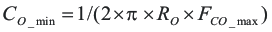
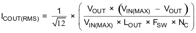
Where RO is the output load impedance (VO/IO) and fCO is the desired crossover frequency. For a desired maximum crossover of 50 kHz the minimum value for the output capacitor is around 2.5 μF. This may not satisfy the output ripple voltage requirement. The output ripple voltage consists of two components; the voltage change due to the charge and discharge of the output filter capacitance and the voltage change due to the ripple current times the ESR of the output filter capacitor. The output ripple voltage can be estimated by:
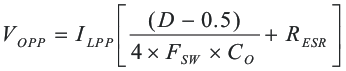
The maximum ESR of the output capacitor can be determined from the amount of allowable output ripple as specified in the initial design parameters. The contribution to the output ripple voltage due to ESR is the inductor ripple current times the ESR of the output filter, so the maximum specified ESR as listed in the capacitor data sheet is given by Equation 14.
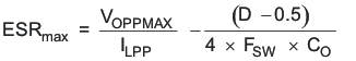
Where VOPPMAX is the desired maximum peak-to-peak output ripple. The maximum RMS ripple current in the output capacitor is given by Equation 15.
Where NC is the number of output capacitors in parallel.
For this design example, a single 22-μF ceramic output capacitor is chosen for C6. It is rated at 10 V with a maximum ESR of 5 mΩ and a ripple current rating in excess of 3 A. The calculated total RMS ripple current is 182 mA and the maximum total ESR required is 51 mΩ. This output capacitor exceeds the requirements by a wide margin and will result in a reliable, high-performance design. it is important to note that the actual capacitance in circuit may be less than the catalog value when the output is operating near the rated voltage for the capacitor. The selected output capacitor must be rated for a voltage greater than the desired output voltage plus ½ the ripple voltage but in this example a 10-V capacitor is used so that the effective capacitance will remain close to the stated value of 22 μF. Other capacitor types work well with the TPS54232, depending on the needs of the application.
9.2.2.5 Compensation Components
The external compensation used with the TPS54232 allows for a wide range of output filter configurations. A large range of capacitor values and types of dielectric are supported. The design example uses a ceramic X5R dielectric output capacitor, but other types are supported.
A Type II compensation scheme is recommended for the TPS54232. The compensation components are chosen to set the desired closed loop cross over frequency and phase margin for output filter components. The type II compensation has the following characteristics; a dc gain component, a low frequency pole, and a mid frequency zero / pole pair.
The DC gain is determined by Equation 16.
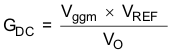
Where:
Vggm = 800
VREF = 0.8 V
The low-frequency pole is determined by Equation 17.
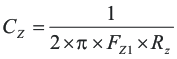
The mid-frequency zero is determined by Equation 18.
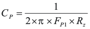
And, the mid-frequency pole is given by Equation 19.
The first step is to choose the closed loop crossover frequency. In general, the closed-loop crossover frequency should be less than 1/8 of the minimum operating frequency, but for the TPS54232 it is recommended that the maximum closed loop crossover frequency be not greater than 75 kHz. Next, the required gain and phase boost of the crossover network needs to be calculated. By definition, the gain of the compensation network must be the inverse of the gain of the modulator and output filter. For this design example, where the ESR zero is much higher than the closed loop crossover frequency, the gain of the modulator and output filter can be approximated by Equation 20.

Where:
FCO = Closed-loop crossover frequency
CO = Output capacitance
The phase loss is given by Equation 21.

Where:
RESR = Equivalent series resistance of the output capacitor
RO = VO/IO
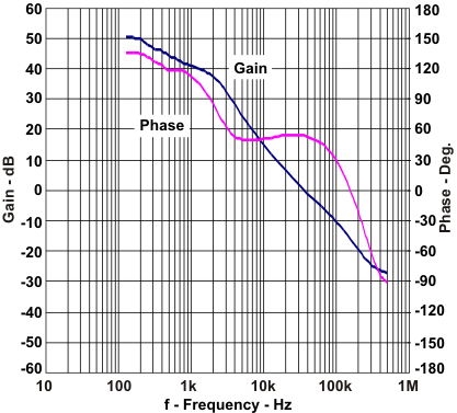
The measured overall loop response for the circuit is given in Figure 20. Note that the actual closed-loop crossover frequency is higher than intended at about 25 kHz. This is primarily due to variation in the actual values of the output filter components and tolerance variation of the internal feed-forward gain circuitry. Overall the design has greater than 60 degrees of phase margin and will be completely stable over all combinations of line and load variability.
Now that the phase loss is known the required amount of phase boost to meet the phase margin requirement can be determined. The required phase boost is given by Equation 22.

Where PM = the desired phase margin.
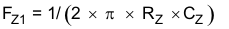
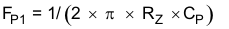
A zero / pole pair of the compensation network will be placed symmetrically around the intended closed loop frequency to provide maximum phase boost at the crossover point. The amount of separation can be determined by Equation 23 and the resultant zero and pole frequencies are given by Equation 24 and Equation 25.

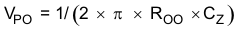
The low-frequency pole is set so that the gain at the crossover frequency is equal to the inverse of the gain of the modulator and output filter. Due to the relationships established by the pole and zero relationships, the value of RZ can be derived directly by Equation 26.
Where:
VO = Output voltage
CO = Output capacitance
FCO = Desired crossover frequency
ROA = 8.696 MΩ
GMCOMP = 10 A/V
Vggm = 800
VREF = 0.8 V
With RZ known, CZ and CP can be calculated using Equation 27 and Equation 28.
For this design, a 22-μF output capacitor issued. For ceramic capacitors, the actual output capacitance is less than the rated value when the capacitors have a dc bias voltage applied. This is the case in a DC - DC converter. For this design, a 10-V capacitor is chosen to minimize this effect. The ESR is approximately 0.005 Ω.
Using Equation 20 and Equation 21, the output stage gain and phase loss are equivalent as:
Gain = 1.613 dB
and
PL = -92.3 degrees
For 60 degrees of phase margin, Equation 22 requires 62.33 degrees of phase boost.
Equation 23, Equation 24, and Equation 25 are used to find the zero and pole frequencies of:
FZ1 = 12.3 k Hz
And
FP1 = 203 kHz
RZ, CZ, and CP are calculated using Equation 26, Equation 27, and Equation 28.

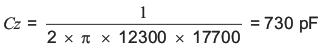
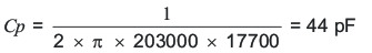
Using standard values for R3, C6, and C7 in the application schematic of Figure 10:
R3 = 17.4 kΩ
C6 = 680 pF
C7 = 47 pF
9.2.2.6 Bootstrap Capacitor
Every TPS54232 design requires a bootstrap capacitor, C4. The bootstrap capacitor must be 0.1 μF. The bootstrap capacitor is located between the PH pins and BOOT pin. The bootstrap capacitor should be a high-quality ceramic type with X7R or X5R grade dielectric for temperature stability.
9.2.2.7 Catch Diode
The TPS54232 is designed to operate using an external catch diode between PH and GND. The selected diode must meet the absolute maximum ratings for the application: Reverse voltage must be higher than the maximum voltage at the PH pin, which is VIN(MAX) + 0.5 V. Peak current must be greater than IOUTMAX plus on half the peak to peak inductor current. Forward voltage drop should be small for higher efficiencies. It is important to note that the catch diode conduction time is typically longer than the high-side FET on time, so attention paid to diode parameters can make a marked improvement in overall efficiency. Additionally, check that the device chosen is capable of dissipating the power losses. For this design, a Diodes, Inc. B220A is chosen, with a reverse voltage of 20 V, forward current of 2 A, and a forward voltage drop of 0.5 V.
9.2.2.8 Output Voltage Limitations
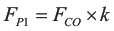
Due to the internal design of the TPS54232, there are both upper and lower output voltage limits for any given input voltage. The upper limit of the output voltage set point is constrained by the maximum duty cycle of 90% and is given by Equation 32.

Where:
VIN(min) = Minimum input voltage
IO(max) = Maximum load current
VD = Catch diode forward voltage
RL = Output inductor series resistance
The equation assumes maximum on resistance for the internal high-side FET.
The lower limit is constrained by the minimum controllable on time which may be as high as 135 ns. The approximate minimum output voltage for a given input voltage and minimum load current is given by Equation 33.

Where:
VIN(max) = Maximum input voltage
IO(min) = Minimum load current
VD = Catch diode forward voltage
RL = Output inductor series resistance
This equation assumes nominal on-resistance for the high-side FET and accounts for worst case variation of operating frequency set point. Any design operating near the operational limits of the device should be carefully checked to assure proper functionality.
9.2.2.9 Power Dissipation Estimate
The following formulas show how to estimate the device power dissipation under continuous conduction mode operations. They should not be used if the device is working in the discontinuous conduction mode (DCM) or pulse-skipping Eco-Mode.
The device power dissipation includes:
- Conduction loss: Pcon = IOUT2 x RDS(on) x VOUT/VIN
- Switching loss: Psw = 0.5 x 10⁻⁹ x VIN2 x IOUT x Fsw
- Gate charge loss: Pgc. = 22.8 x 10⁻⁹ x Fsw
- Quiescent current loss: Pq = 0.085 x 10⁻³ x VIN
Where:
IOUT is the output current (A).
RDS(on) is the on-resistance of the high-side MOSFET (Ω).
VOUT is the output voltage (V).
VIN is the input voltage (V).
Fsw is the switching frequency (Hz).
So:
Ptot = Pcon + Psw + Pgc + Pq
For given TA , TJ = TA + Rth x Ptot.
For given TJMAX = 150°C, TAMAX = TJMAX– Rth x Ptot.
Where:
Ptot is the total device power dissipation (W).
TA is the ambient temperature (°C).
TJ is the junction temperature (°C) .
Rth is the thermal resistance of the package (°C/W).
TJMAX is maximum junction temperature (°C).
TAMAX is maximum ambient temperature (°C).
9.2.3 Application Curves
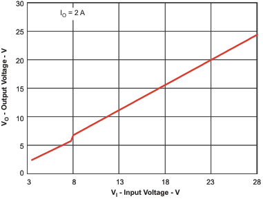
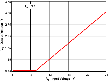 Figure 11. Typical Minimum Output Voltage vs Input Voltage
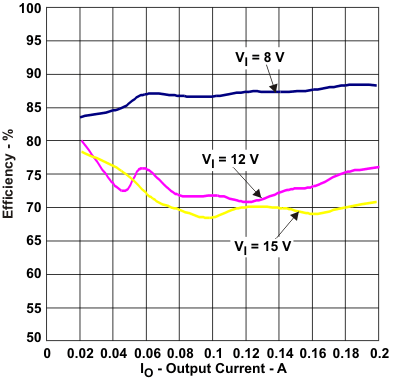
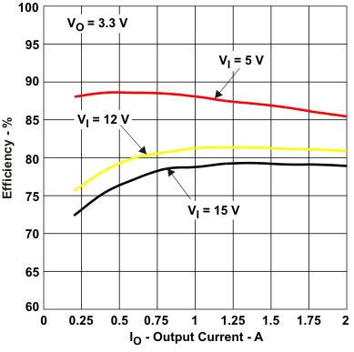 Figure 13. TPS54232 Efficiency
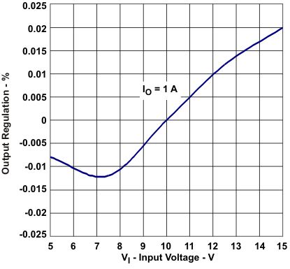
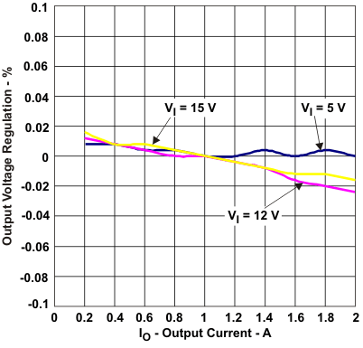 Figure 15. TPS54232 Load Regulation
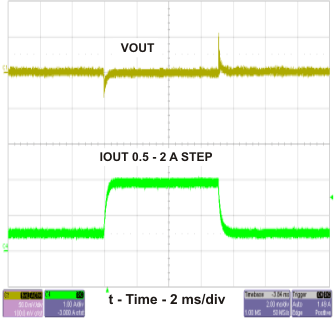 Figure 17. TPS54232 Transient Response
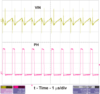
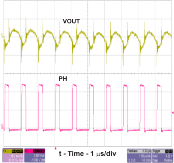 Figure 19. TPS54232 Output Ripple
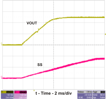
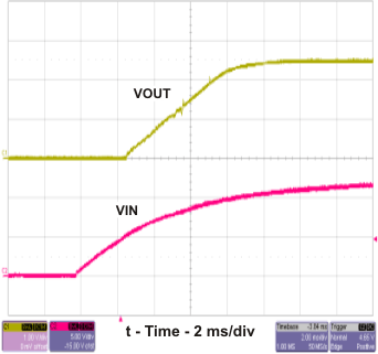 Figure 21. TPS54232 Startup