SLVS876D November 2008 – November 2014 TPS54232
PRODUCTION DATA.
- 1 Features
- 2 Applications
- 3 Description
- 4 Simplified Schematic
- 5 Revision History
- 6 Pin Configuration and Functions
- 7 Specifications
-
8 Detailed Description
- 8.1 Overview
- 8.2 Functional Block Diagram
- 8.3
Feature Description
- 8.3.1 Fixed-Frequency PWM Control
- 8.3.2 Voltage Reference (Vref)
- 8.3.3 Bootstrap Voltage (BOOT)
- 8.3.4 Enable and Adjustable Input Undervoltage Lockout (VIN UVLO)
- 8.3.5 Programmable Slow-Start Using SS Pin
- 8.3.6 Error Amplifier
- 8.3.7 Slope Compensation
- 8.3.8 Current Mode Compensation Design
- 8.3.9 Overcurrent Protection and Frequency Shift
- 8.3.10 Overvoltage Transient Protection
- 8.3.11 Thermal Shutdown
- 8.4 Device Functional Modes
-
9 Application and Implementation
- 9.1 Application Information
- 9.2
Typical Application
- 9.2.1 Design Requirements
- 9.2.2 Detailed Design Procedure
- 9.2.3 Application Curves
- 10Power Supply Recommendations
- 11Layout
- 12Device And Documentation Support
- 13Mechanical, Packaging, And Orderable Information
8 Detailed Description
8.1 Overview
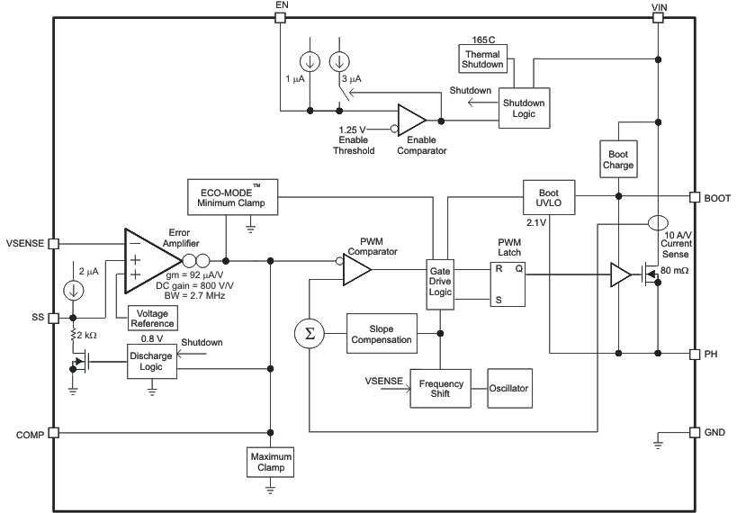
The TPS54232 is a 28-V, 2-A, step-down (buck) converter with an integrated high-side n-channel MOSFET. To improve performance during line and load transients, the device implements a constant frequency, current mode control which reduces output capacitance and simplifies external frequency compensation design. The TPS54232 has a pre-set switching frequency of 1MHz.
The TPS54232 needs a minimum input voltage of 3.5 V to operate normally. The EN pin has an internal pull-up current source that can be used to adjust the input-voltage, undervoltage lockout (UVLO) with two external resistors. In addition, the pull-up current provides a default condition when the EN pin is floating for the device to operate. The operating current is 85 μA typically when not switching and under no load. When the device is disabled, the supply current is 1 μA typically.
The integrated 80-mΩ high-side MOSFET allows for high efficiency power supply designs with continuous output currents up to 2 A.
The TPS54232 reduces the external component count by integrating the boot recharge diode. The bias voltage for the integrated high-side MOSFET is supplied by an external capacitor on the BOOT to PH pin. The boot capacitor voltage is monitored by an UVLO circuit and will turn the high-side MOSFET off when the voltage falls below a preset threshold of 2.1 V typically. The output voltage can be stepped down to as low as the reference voltage.
By adding an external capacitor, the slow start time of the TPS54232 can be adjustable which enables flexible output filter selection.
To improve the efficiency at light load conditions, the TPS54232 enters a special pulse-skipping Eco-Mode when the peak inductor current drops below 100 mA typically.
The frequency foldback reduces the switching frequency during startup and over current conditions to help control the inductor current. The thermal shut down gives the additional protection under fault conditions.
8.2 Functional Block Diagram
8.3 Feature Description
8.3.1 Fixed-Frequency PWM Control
The TPS54232 uses a fixed frequency, peak current mode control. The internal switching frequency of the TPS54232 is fixed at 1 MHz.
8.3.2 Voltage Reference (Vref)
The voltage reference system produces a ±2% initial accuracy voltage reference (±3.5% over temperature) by scaling the output of a temperature stable bandgap circuit. The typical voltage reference is designed at 0.8 V.
8.3.3 Bootstrap Voltage (BOOT)
The TPS54232 has an integrated boot regulator and requires a 0.1-μF ceramic capacitor between the BOOT and PH pin to provide the gate drive voltage for the high-side MOSFET. A ceramic capacitor with an X7R or X5R grade dielectric is recommended because of the stable characteristics over temperature and voltage. To improve drop out, the TPS54232 is designed to operate at 100% duty cycle as long as the BOOT to PH pin voltage is greater than 2.1 V typically.
8.3.4 Enable and Adjustable Input Undervoltage Lockout (VIN UVLO)
The EN pin has an internal pull-up current source that provides the default condition of the TPS54232 operating when the EN pin floats.
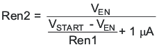
The TPS54232 is disabled when the VIN pin voltage falls below internal VIN UVLO threshold. It is recommended to use an external VIN UVLO to add hysteresis unless VIN is greater than (VOUT + 2V). To adjust the VIN UVLO with hysteresis, use the external circuitry connected to the EN pin as shown in Figure 9. Once the EN pin voltage exceeds 1.25 V, an additional 3 μA of hysteresis is added. Use Equation 1 and Equation 2 to calculate the resistor values needed for the desired VIN UVLO threshold voltages. The VSTART is the input start threshold voltage, the VSTOP is the input stop threshold voltage and the VEN is the enable threshold voltage of 1.25 V. The VSTOP should always be greater than 3.5 V.
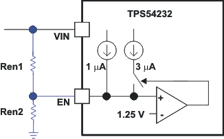 Figure 9. Adjustable Input Undervoltage Lockout

8.3.5 Programmable Slow-Start Using SS Pin
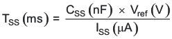
It is highly recommended to program the slow start time externally because no slow start time is implemented internally. The TPS54232 effectively uses the lower voltage of the internal voltage reference or the SS pin voltage as the power supply’s reference voltage fed into the error amplifier and will regulate the output accordingly. A capacitor (CSS) on the SS pin to ground implements a slow start time. The TPS54232 has an internal pull-up current source of 2 μA that charges the external slow start capacitor. The equation for the slow start time (10% to 90%) is shown in Equation 3. The Vref is 0.8V and the ISS current is 2μA.
The slow start time should be set between 1 ms to 10 ms to ensure good startup behavior. The slow-start capacitor should be no more than 27 nF.
If during normal operation, the input voltage drops below the VIN UVLO threshold, or the EN pin is pulled below 1.25 V, or a thermal shutdown event occurs, the TPS54232 stops switching.
8.3.6 Error Amplifier
The TPS54232 has a transconductance amplifier for the error amplifier. The error amplifier compares the VSENSE voltage to the internal effective voltage reference presented at the input of the error amplifier. The transconductance of the error amplifier is 92 μA/V during normal operation. Frequency compensation components are connected between the COMP pin and ground.
8.3.7 Slope Compensation
In order to prevent the sub-harmonic oscillations when operating the device at duty cycles greater than 50%, the TPS54232 adds a built-in slope compensation which is a compensating ramp to the switch current signal.
8.3.8 Current Mode Compensation Design
For designs using ceramic output capacitors, proper derating of ceramic output capacitance is recommended when doing the stability analysis. This is because the actual ceramic capacitance drops considerably from the nominal value when the applied voltage increases. For the detailed guidelines, see the section.
8.3.9 Overcurrent Protection and Frequency Shift
The TPS54232 implements current mode control that uses the COMP pin voltage to turn off the high-side MOSFET on a cycle by cycle basis. Every cycle the switch current and the COMP pin voltage are compared; when the peak inductor current intersects the COMP pin voltage, the high-side switch is turned off. During overcurrent conditions that pull the output voltage low, the error amplifier responds by driving the COMP pin high, causing the switch current to increase. The COMP pin has a maximum clamp internally, which limit the output current.
The TPS54232 provides robust protection during short circuits. There is potential for overcurrent runaway in the output inductor during a short circuit at the output. The TPS54232 solves this issue by increasing the off time during short circuit conditions by lowering the switching frequency. The switching frequency is divided by 8, 4, 2, and 1 as the voltage ramps from 0 V to 0.8 V on VSENSE pin. The relationship between the switching frequency and the VSENSE pin voltage is shown in Table 1.
Table 1. Switching Frequency Conditions
| SWITCHING FREQUENCY | VSENSE PIN VOLTAGE |
|---|---|
| 1 MHz | VSENSE ≥ 0.6 V |
| 1 MHz / 2 | 0.6 V > VSENSE ≥ 0.4 V |
| 1 MHz / 4 | 0.4 V > VSENSE ≥ 0.2 V |
| 1 MHz / 8 | 0.2 V > VSENSE |
8.3.10 Overvoltage Transient Protection
The TPS54232 incorporates an overvoltage transient protection (OVTP) circuit to minimize output voltage overshoot when recovering from output fault conditions or strong unload transients. The OVTP circuit includes an overvoltage comparator to compare the VSENSE pin voltage and internal thresholds. When the VSENSE pin voltage goes above 109% × Vref, the high-side MOSFET will be forced off. When the VSENSE pin voltage falls below 107% × Vref, the high-side MOSFET will be enabled again.
8.3.11 Thermal Shutdown
The device implements an internal thermal shutdown to protect itself if the junction temperature exceeds 165°C. The thermal shutdown forces the device to stop switching when the junction temperature exceeds the thermal trip threshold. Once the die temperature decreases below 165°C, the device reinitiates the power up sequence.
8.4 Device Functional Modes
8.4.1 Eco-Mode
The TPS54232 device is designed to operate in pulse skipping Eco-mode at light load currents to boost light load efficiency. When the peak inductor current is lower than 100 mA (typical), the COMP pin voltage falls to 0.5 V (typical) and the device enters Eco-mode . When the device is in Eco-mode, the COMP pin voltage is clamped at 0.5 V internally which prevents the high-side integrated MOSFET from switching. The peak inductor current must rise above 100 mA for the COMP pin voltage to rise above 0.5 V and exit Eco-mode. Because the integrated current comparator catches the peak inductor current only, the average load current entering Eco-mode varies with the applications and external output filters.
8.4.2 Operation With VIN < 3.5 V
The device is recommended to operate with input voltages above 3.5 V. The typical VIN UVLO threshold is not specified and the device can operate at input voltages down to the UVLO voltage. At input voltages below the actual UVLO voltage, the device does not switch. If the EN pin is externally pulled up or left floating, the device becomes active when the VIN pin passes the UVLO threshold. Switching begins when the slow-start sequence is initiated.
8.4.3 Operation With EN Control
The enable threshold voltage is 1.25 V (typical). With the EN pin is held below that voltage the device is disabled and switching is inhibited even if the VIN pin is above the UVLO threshold. The IC quiescent current is reduced in this state. If the EN voltage increases above the threshold while the VIN pin is above the UVLO threshold, the device becomes active. Switching is enabled, and the slow-start sequence is initiated.