SLVS885I October 2008 – December 2017 TPS23754 , TPS23754-1 , TPS23756
PRODUCTION DATA.
- 1 Features
- 2 Applications
- 3 Description
- 4 Revision History
- 5 Pin Configuration and Functions
- 6 Specifications
-
7 Detailed Description
- 7.1 Overview
- 7.2 Functional Block Diagram
- 7.3 Feature Description
- 7.4
Device Functional Modes
- 7.4.1
PoE Overview
- 7.4.1.1 Threshold Voltages
- 7.4.1.2 PoE Start-Up Sequence
- 7.4.1.3 Detection
- 7.4.1.4 Hardware Classification
- 7.4.1.5 Inrush and Start-Up
- 7.4.1.6 Maintain Power Signature
- 7.4.1.7 Start-Up and Converter Operation
- 7.4.1.8 PD Hotswap Operation
- 7.4.1.9 Converter Controller Features
- 7.4.1.10 Bootstrap Topology
- 7.4.1.11 Current Slope Compensation and Current Limit
- 7.4.1.12 Blanking – RBLNK
- 7.4.1.13 Dead Time
- 7.4.1.14 FRS and Synchronization
- 7.4.1.15 T2P, Start-Up, and Power Management
- 7.4.1.16 Thermal Shutdown
- 7.4.1.17 Adapter ORing
- 7.4.1.18 PPD ORing Features
- 7.4.1.19 Using DEN to Disable PoE
- 7.4.1.20 ORing Challenges
- 7.4.1
PoE Overview
-
8 Application and Implementation
- 8.1 Application Information
- 8.2
Typical Application
- 8.2.1 Design Requirements
- 8.2.2
Detailed Design Procedure
- 8.2.2.1 Input Bridges and Schottky Diodes
- 8.2.2.2 Protection, D1
- 8.2.2.3 Capacitor, C1
- 8.2.2.4 Detection Resistor, RDEN
- 8.2.2.5 Classification Resistor, RCLS
- 8.2.2.6 Dead Time Resistor, RDT
- 8.2.2.7 Switching Transformer Considerations and RVC
- 8.2.2.8 Special Switching MOSFET Considerations
- 8.2.2.9 Thermal Considerations and OTSD
- 8.2.2.10 APD Pin Divider Network, RAPD1, RAPD2
- 8.2.2.11 PPD Pin Divider Network, RPPD1, RPPD2
- 8.2.2.12 Setting Frequency (RFRS) and Synchronization
- 8.2.2.13 Current Slope Compensation
- 8.2.2.14 Blanking Period, RBLNK
- 8.2.2.15 Estimating Bias Supply Requirements and CVC
- 8.2.2.16 T2P Pin Interface
- 8.2.2.17 Advanced ORing Techniques
- 8.2.2.18 Soft Start
- 8.2.2.19 Frequency Dithering for Conducted Emissions Control
- 8.2.3 Application Curves
- 9 Power Supply Recommendations
- 10Layout
- 11Device and Documentation Support
- 12Mechanical, Packaging, and Orderable Information
8.2.2.16 T2P Pin Interface
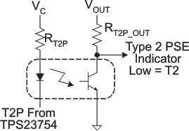
The T2P pin is an active low, open-drain output indicating a high-power source is available. An optocoupler is typically used to interface with the T2P pin to signal equipment on the secondary side of the converter of T2P status. Optocoupler current-gain is referred to as current transfer ratio (CTR), which is the ratio of transistor collector current to LED current. To preserve efficiency, TI recommends a high-gain optocoupler ( 250% ≤ CTR ≤ 500%, or 300% ≤ CTR ≤ 600% ) along with a high-impedance (for example, CMOS) receiver. Design of the T2P optocoupler interface can be accomplished as follows:
 Figure 32. T2P Interface
- T2P ON characteristic: IT2P = 2 mA minimum, VT2P = 1 V
- Let VC = 12 V, VOUT = 5 V, RT2P-OUT = 10 kΩ, VT2P-OUT (low) = 400 mV maximum
- The optocoupler CTR will be needed to determine RT2P. A device with a minimum CTR of 300% at 5-mA LED bias current is selected. CTR will also vary with temperature and LED bias current. The strong variation of CTR with diode current makes this a problem that requires some iteration using the CTR versus IDIODE curve on the optocoupler data sheet.
- Using the (normalized) curves, a current of 0.4 to 0.5 mA is required to support the output current at the minimum CTR at 25°C.
- Pick an IDIODE. For example one around the desired load current.
- Use the optocoupler data sheet curve to determine the effective CTR at this operating current. It is usually necessary to apply the normalized curve value to the minimum specified CTR. It might be necessary to ratio or offset the curve readings to obtain a value that is relative to the current that the CTR is specified at.
- If IDIODE × CTRI_DIODE is substantially different from IRT2P_OUT, choose another IDIODE and repeat.
- This manufacturer’s curves also indicate a –20% variation of CTR with temperature. The approximate forward voltage of the optocoupler diode is 1.1 V from the data sheet.

- VFLED ≉ 1.1 V

- Select a 15.4-kΩ resistor. Even though the minimum CTR and temperature variation were considered, the designer might choose a smaller resistor for a little more margin.
- Using the (normalized) curves, a current of 0.4 to 0.5 mA is required to support the output current at the minimum CTR at 25°C.
