SLVSBA4F June 2012 – April 2021 DRV8837 , DRV8838
PRODUCTION DATA
- 1 Features
- 2 Applications
- 3 Description
- 4 Revision History
- 5 Pin Configuration and Functions
- 6 Specifications
- 7 Detailed Description
- 8 Power Supply Recommendations
- 9 Layout
- 10Device and Documentation Support
7.3.2 Independent Half-Bridge Control
The control logic for independent half-bridge drive is shown in Table 7-3. Columns INx and OUTx show the original logic of the DRV8837. Note that although a swap is included in this implementation, it is still valid that Cx = 1 spins a motor or energizes a solenoid connected at corresponding Mx, while Cx = 0, stops the motor or discharges the solenoid.
| C1 | C2 | IN1 | IN2 | OUT1 | OUT2 | M1 | M2 |
|---|---|---|---|---|---|---|---|
| 0 | 0 | 0 | 0 | Z | Z | Off: Braking mode 1 | Off: Braking mode 1 |
| 1 | 0 | 0 | 1 | L | H | On: Driving mode | Off: Braking mode 2 |
| 0 | 1 | 1 | 0 | H | L | Off: Braking mode 2 | On: Driving mode |
| 1 | 1 | 1 | 1 | L | L | On: Driving mode | On: Driving mode |
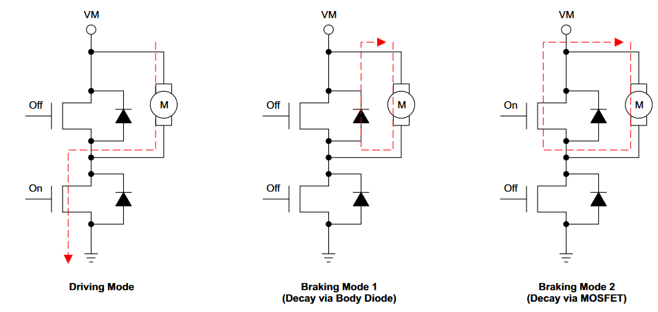
Figure 7-4 shows the driving mode and the two current decay paths during current regulation when PWM input control is used. The driving mode occurs when the corresponding half-bridge Cx signal is HIGH. When the Cx signal is LOW, the corresponging half bridge can go into either braking mode 1 or braking mode 2. In braking mode 1, both the high- and low-side MOSFETs of the half-bridge are tri-stated, and the recirculation current flows through the body diode of the high-side MOSFET as well as the motor itself. This braking mode happens when both C1 and C2 are LOW. If one of the Cx input is LOW and the other HIGH, the half-bridge corresponding to the LOW Cx input will go into braking mode 2. In braking mode 2, the low-side FET is OFF while its high-side counterpart is ON. The recirculation current flows through the high-side MOSFET and the motor.
 Figure 7-4 Normal Driving and Current
Decay Modes
Figure 7-4 Normal Driving and Current
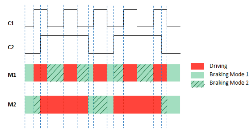
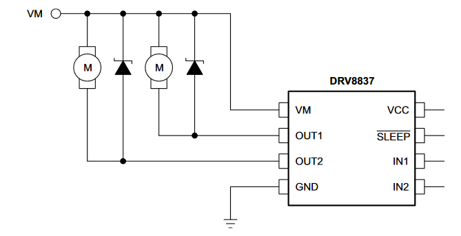
Decay ModesWhen each of the Cx inputs are independently controlled with different PWM frequencies and duty cycle, each half-bridge will go into a combination of braking mode 1 and braking mode 2. Figure 7-5 show a driving and decay example with independent PWM inputs. If the half-bridge spends more time in braking mode 1, the motor average speed will be lower since more power is dissipated through the MOSFET body diode. To reduce the power dissipated during braking mode 1, it is recommended to placed Schottky diodes with forward voltage less than 0.6V across the motors as shown in Figure 7-6. Note that if On/Off control mode (constant HIGH or LOW at inputs) is used, the two braking modes do not interact with each other and hence have no effect on the average speed of the two motors.
 Figure 7-5 Driving and Decay Examples
with Independent PWM Inputs
 Figure 7-6 Improved Application
Circuit for Better Motor Performance