SLVSBR3A May 2013 – June 2015 TPS61158
PRODUCTION DATA.
- 1 Features
- 2 Applications
- 3 Description
- 4 Revision History
- 5 Pin Configuration and Functions
- 6 Specifications
- 7 Detailed Description
- 8 Application and Implementation
- 9 Power Supply Recommendations
- 10Layout
- 11Device and Documentation Support
- 12Mechanical, Packaging, and Orderable Information
6 Specifications
6.1 Absolute Maximum Ratings
over operating free-air temperature range (unless otherwise noted)(1)| MIN | MAX | UNIT | ||
|---|---|---|---|---|
| Voltage range(2) | VIN | –0.3 | 6 | V |
| VOUT, LX | –0.3 | 30 | V | |
| FB, CTRL | –0.3 | 7 | V | |
| Continuous power dissipation | ||||
| Operating junction temperature | –40 | 150 | °C | |
| Storage temperature, Tstg | –65 | 150 | °C | |
(1) Stresses beyond those listed under Absolute Maximum Ratings may cause permanent damage to the device. These are stress ratings only, which do not imply functional operation of the device at these or any other conditions beyond those indicated under Recommended Operating Conditions. Exposure to absolute-maximum-rated conditions for extended periods may affect device reliability.
(2) All voltage values are with respect to network ground terminal.
6.2 ESD Ratings
| VALUE | UNIT | |||
|---|---|---|---|---|
| V(ESD) | Electrostatic discharge | Human-body model (HBM), per ANSI/ESDA/JEDEC JS-001(1) | ±2000 | V |
| Charged-device model (CDM), per JEDEC specification JESD22-C101(2) | ±500 | |||
(1) JEDEC document JEP155 states that 500-V HBM allows safe manufacturing with a standard ESD control process.
(2) JEDEC document JEP157 states that 250-V CDM allows safe manufacturing with a standard ESD control process.
6.3 Recommended Operating Conditions
over operating free-air temperature range (unless otherwise noted)| MIN | NOM | MAX | UNIT | ||
|---|---|---|---|---|---|
| VIN | Input voltage | 2.7 | 5.5 | V | |
| VOUT | Output voltage | VIN | 29 | V | |
| IOUT | Output load current | 30 | mA | ||
| L | Inductor | 10 | 22 | µH | |
| CI | Input capacitor | 1 | 10 | µF | |
| CO | Output capacitor | 0.47 | 2.2 | µF | |
| FPWM | Input PWM signal frequency | 20 | 100 | kHz | |
| TA | Operating ambient temperature | –40 | 85 | °C | |
| TJ | Operating junction temperature | –40 | 125 | °C | |
6.4 Thermal Information
| THERMAL METRIC(1) | TPS61158 | UNIT | |
|---|---|---|---|
| DRV (WSON) | |||
| 6 PINS | |||
| RθJA | Junction-to-ambient thermal resistance | 70.4 | °C/W |
| RθJC(top) | Junction-to-case (top) thermal resistance | 94.8 | °C/W |
| RθJB | Junction-to-board thermal resistance | 39.8 | °C/W |
| ψJT | Junction-to-top characterization parameter | 2.5 | °C/W |
| ψJB | Junction-to-board characterization parameter | 40.2 | °C/W |
| RθJC(bot) | Junction-to-case (bottom) thermal resistance | 10.2 | °C/W |
(1) For more information about traditional and new thermal metrics, see the Semiconductor and IC Package Thermal Metrics application report, SPRA953.
6.5 Electrical Characteristics
VIN = 3.6 V, CTRL = High, IFB current = 20 mA, IFB voltage = 200 mV, TA = –40°C to 85°C, typical values are at TA = 25°C (unless otherwise noted).| PARAMETER | TEST CONDITIONS | MIN | TYP | MAX | UNIT | |
|---|---|---|---|---|---|---|
| POWER SUPPLY | ||||||
| VIN | Input voltage range | 2.7 | 5.5 | V | ||
| VIN_UVLO | VIN undervoltage lockout threshold | VIN ramp down | 2.2 | 2.35 | V | |
| VIN ramp up | 2.5 | 2.65 | ||||
| VIN_HYS | VIN undervoltage lockout hysteresis | 275 | mV | |||
| IQ | Operating quiescent current into VIN | Device enable, no switching and no load (VFB = 0.4 V) | 0.3 | 0.5 | mA | |
| Device enable, switching 750 kHz and no load (VFB = 0 V) |
0.5 | 1.65 | ||||
| ISD | Shutdown current | CTRL = GND | 0.1 | 1 | µA | |
| CONTROL LOGIC AND TIMING | ||||||
| VH | CTRL logic high voltage | 1.2 | V | |||
| VL | CTRL logic Low voltage | 0.4 | V | |||
| RPD | CTRL pin internal pull-down resistor | VCTRL = 1.8 V | 300 | kΩ | ||
| tSD | CTRL pulse width to shutdown | CTRL from high to low | 3.5 | ms | ||
| VOLTAGE AND CURRENT REGULATION | ||||||
| VREF | Voltage feedback regulation voltage | Duty = 100% | 194 | 200 | 206 | mV |
| IFB | FB pin bias current | VFB = 200 mV | 2 | µA | ||
| tREF | VREF filter time constant | 230 | µs | |||
| POWER SWITCH AND DIODE | ||||||
| RDS(ON) | N-channel MOSFET on-resistance | VIN = 3.6 V, TA = 25°C, IOUT = 100 mA |
0.6 | 1 | Ω | |
| VF | Power diode forward voltage | IDIODE = 0.2 A | 0.75 | 1 | V | |
| ILEAK_LX | LX pin leakage current | VLX = 28 V | 0.1 | 2 | µA | |
| OSCILLATOR | ||||||
| ƒSW | Oscillator frequency | 600 | 750 | 900 | kHz | |
| Dmax | Maximum duty cycle of boost switching | VFB = 0 V, measured on the drive signal of the switch MOSFET | 88% | 94% | ||
| PROTECTION AND SOFT START | ||||||
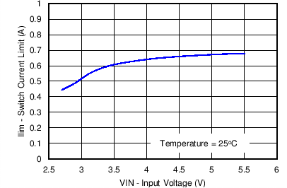
| ILIM | NMOS current limit | VIN = 3.6 V, D = DMAX
TA = 0°C to 85°C |
0.5 | 0.6 | 0.7 | A |
| ILIM_Start | Start up current limit | 360 | mA | |||
| tILIM_Start | Time step for start up current limit | 8 | ms | |||
| VOVP | Open LED protection threshold | Tested at VOUT pin | 27.5 | 28.2 | 29 | V |
| VACKNL | Acknowledge output voltage low | Open drain, Rpullup = 15 kΩ to VIN | 0.4 | V | ||
| THERMAL SHUTDOWN | ||||||
| Tshutdown | Thermal shutdown threshold | 160 | °C | |||
| Thys | Thermal shutdown hysteresis | 15 | °C | |||
6.6 EasyScale Timing Requirements
| MIN | NOM | MAX | UNIT | ||
|---|---|---|---|---|---|
| tes_detect | EasyScale detection time(1), CTRL low | 450 | µs | ||
| tes_delay | EasyScale detection delay | 100 | µs | ||
| tes_win | EasyScale detection window time, measured from CTRL high | 3.5 | ms | ||
| tstart | Start time of program stream | 3.5 | µs | ||
| tEOS | End time of program stream | 3.5 | 600 | µs | |
| tH_LB | High time of low bit, Logic 0 | 3.5 | 300 | µs | |
| tL_LB | Low time of low bit, Logic 0 | 2 × tH_LB | 600 | µs | |
| tH_HB | High time of high bit, Logic 1 | 2 × tL_HB | 600 | µs | |
| tL_HB | Low time of high bit, Logic 1 | 3.5 | 300 | µs | |
| tvalACK | Acknowledge valid time (see(2)) | 3.5 | µs | ||
| tACKN | Duration of acknowledge condition (see(2)) | 900 | µs | ||
(1) To select EasyScale mode, the CTRL pin has to be low for more than tes_detect during tes_win
(2) Acknowledge condition active 0, this condition will only be applied in case the RFA bit is set. Open drain output, line needs to be pulled high by the host with resistor load.
6.7 Typical Characteristics
