SLVSDQ0J september   2017  – august 2023 TPS7B82-Q1

PRODUCTION DATA  

  1.   1
  2. Features
  3. Applications
  4. Description
  5. Revision History
  6. Pin Configuration and Functions
  7. Specifications
    1. 6.1 Absolute Maximum Ratings
    2. 6.2 ESD Ratings
    3. 6.3 Recommended Operating Conditions
    4. 6.4 Thermal Information
    5. 6.5 Electrical Characteristics: Grade 1 Options
    6. 6.6 Electrical Characteristics: Grade 0 Options
    7. 6.7 Typical Characteristics
  8. Detailed Description
    1. 7.1 Overview
    2. 7.2 Functional Block Diagram
    3. 7.3 Feature Description
      1. 7.3.1 Device Enable (EN)
      2. 7.3.2 Undervoltage Shutdown
      3. 7.3.3 Current Limit
      4. 7.3.4 Thermal Shutdown
    4. 7.4 Device Functional Modes
      1. 7.4.1 Operation With VIN Lower Than 3 V
      2. 7.4.2 Operation With VIN Larger Than 3 V
  9. Application and Implementation
    1. 8.1 Application Information
    2. 8.2 Typical Application
      1. 8.2.1 Design Requirements
      2. 8.2.2 Detailed Design Procedure
        1. 8.2.2.1 Input Capacitor
        2. 8.2.2.2 Output Capacitor
      3. 8.2.3 Application Curve
    3. 8.3 Power Supply Recommendations
    4. 8.4 Layout
      1. 8.4.1 Layout Guidelines
      2. 8.4.2 Layout Example
  10. Device and Documentation Support
    1. 9.1 Receiving Notification of Documentation Updates
    2. 9.2 Support Resources
    3. 9.3 Trademarks
    4. 9.4 Electrostatic Discharge Caution
    5. 9.5 Glossary
  11. 10Mechanical, Packaging, and Orderable Information

Typical Characteristics

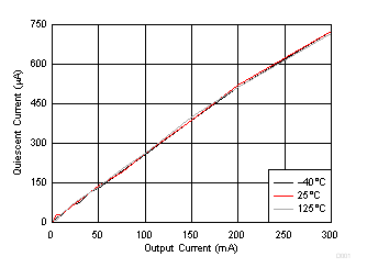
VIN = 14 V, VEN ≥ 2 V, TJ = –40°C to 150°C (unless otherwise noted)
GUID-EA6C54D7-8165-46CA-A7B2-EE02885505AD-low.gif
VOUT = 5 V
Figure 6-1 Quiescent Current vs Output Current
GUID-C62FA36D-75DE-4109-B06B-71D0959EA6C4-low.gif
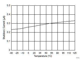
VEN = 0 V
Figure 6-3 Shutdown Current vs Ambient Temperature
GUID-7667D328-82CE-487B-9AF2-F7E9B2C507BE-low.gif
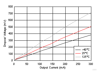
VIN = 5 V, 5-V fixed output, V(Dropout) = VIN – VOUT
Figure 6-5 Dropout Voltage vs Output Current
GUID-C5E5E46D-670D-485D-B3B8-D2FD10943F22-low.gif
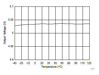
VOUT = 5 V
Figure 6-7 Output Voltage vs Ambient Temperature
GUID-BDC5659C-60B8-478F-BCB5-FB069F702034-low.gif
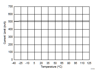
VIN = 14 V, VOUT is shorted to 90% × VOUT
Figure 6-9 Output Current Limit vs Ambient Temperature
GUID-845571C8-976F-4925-8E4A-D4FCEFA7848C-low.gif
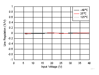
VOUT = 5 V, IOUT = 10 mA
Figure 6-11 Line Regulation
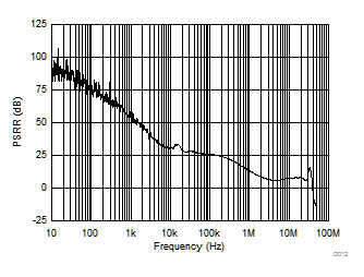
GUID-59355CCC-4C9F-4024-8BA3-65AC106948CF-low.gif
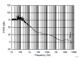
IOUT = 100 mA
Figure 6-13 PSRR vs Frequency
GUID-BA9EB37F-56FE-4996-A635-09337EEDF0DE-low.gif
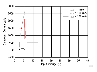
VOUT = 5 V
Figure 6-2 Quiescent Current vs Input Voltage
GUID-EF0AAD6C-0501-4970-BF0A-610688D35010-low.gif
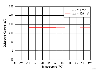
VOUT = 5 V
Figure 6-4 Quiescent Current vs Ambient Temperature
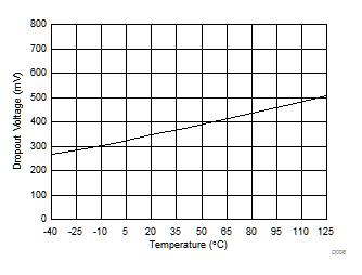
GUID-332E446E-5D0C-4DB2-BC51-CF9A398E23C7-low.gif
VIN = 5 V, 5-V fixed output, V(Dropout) = VIN – VOUT
Figure 6-6 Dropout Voltage vs Ambient Temperature
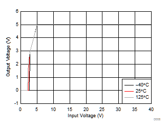
GUID-56F3F02B-DCCB-43C4-B486-329F243E8E2A-low.gif
VOUT = 5 V, IOUT = 1 mA
Figure 6-8 Output Voltage vs Input Voltage
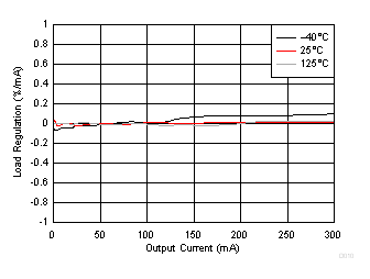
GUID-63C9D5EB-37FD-40A2-93AA-C19F1D203BE1-low.gif
VOUT = 5 V
Figure 6-10 Load Regulation
GUID-2631754F-276C-4AC5-8B60-7A1DC71F3880-low.gif
IOUT = 10 mA
Figure 6-12 PSRR vs Frequency
GUID-5473A7DC-83FB-4998-BC20-FDE8EA73375A-low.gif
 
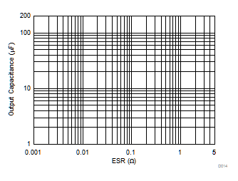
Figure 6-14 Output Capacitance vs ESR Stability