SLVSDV6C November 2017 – November 2019 TPS62821 , TPS62822 , TPS62823
PRODUCTION DATA.
- 1 Features
- 2 Applications
- 3 Description
- 4 Revision History
- 5 Device Comparison Table
- 6 Pin Configuration and Functions
- 7 Specifications
- 8 Detailed Description
- 9 Application and Implementation
- 10Power Supply Recommendations
- 11Layout
- 12Device and Documentation Support
- 13Mechanical, Packaging, and Orderable Information
9.2.2.5 Inductor Selection
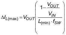
The TPS6282x is designed to work with inductors of 470nH nominal and can be used with 1µH inductors as well. The inductor has to be selected for adequate saturation current and a low dc resistance (DCR). The minimum inductor current rating, that is needed under static load conditions is calculated using Equation 6 and Equation 7.
space

space

space
This calculation gives the minimum saturation current of the inductor needed and an additional margin is recommended to cover dynamic overshoot due to startup or load transients. Inductors are available in different dimensions. Choosing the smallest size might result in less efficiency due to larger DCR and ac losses. The following inductors have been tested with the TPS6282x:
Table 4. List of Recommended Inductors
| TYPE | Nominal INDUCTANCE (1) | Saturation Current and DC Resistance | Dimensions [mm] | Manufacturer(3) | |
|---|---|---|---|---|---|
| max. ISAT [A](2) | max. RDC [mΩ] | ||||
| HTEN20161T-R47MDR | 0.47 | 4.8 | 32 | 2.0 x 1.6 x 1.0 | Cyntec |
| HTEH20121T-R47MSR | 0.47 | 4.6 | 25 | 2.0 x 1.2 x 1.0 | Cyntec |
| DFE201610E - R47M | 0.47 | 4.8 | 32 | 2.0 x 1.6 x 1.0 | muRata |
| DFE201210S - R47M | 0.47 | 4.8 | 32 | 2.0 x 1.2 x 1.0 | muRata |
| TFM201610ALM-R47MTAA | 0.47 | 5.1 | 34 | 2.0 x 1.6 x 1.0 | TDK |
| TFM201610ALC-R47MTAA | 0.47 | 5.2 | 25 | 2.0 x 1.6 x 1.0 | TDK |
| XFL4015-471ME | 0.47 | 6.6 | 8.36 | 4.0 x 4.0 x 1.6 | Coilcraft |