SLVSDV6C November   2017  – November 2019 TPS62821 , TPS62822 , TPS62823

PRODUCTION DATA.  

  1. Features
  2. Applications
  3. Description
    1.     Device Images
      1.      Typical Application Schematic space space space space
      2.      Efficiency vs Output Current space
  4. Revision History
  5. Device Comparison Table
  6. Pin Configuration and Functions
    1.     Pin Functions
  7. Specifications
    1. 7.1 Absolute Maximum Ratings
    2. 7.2 ESD Ratings
    3. 7.3 Recommended Operating Conditions
    4. 7.4 Thermal Information
    5. 7.5 Electrical Characteristics
    6. 7.6 Typical Characteristics
  8. Detailed Description
    1. 8.1 Overview
    2. 8.2 Functional Block Diagram
    3. 8.3 Feature Description
      1. 8.3.1 Enable / Shutdown and Output Discharge
      2. 8.3.2 Soft-Start
      3. 8.3.3 Power Good (PG)
      4. 8.3.4 Undervoltage Lockout (UVLO)
      5. 8.3.5 Thermal Shutdown
    4. 8.4 Device Functional Modes
      1. 8.4.1 Pulse Width Modulation (PWM) Operation
      2. 8.4.2 Power Save Mode (PSM) Operation
      3. 8.4.3 Minimum Duty Cycle and 100% Mode Operation
      4. 8.4.4 Current Limit and Short Circuit Protection
  9. Application and Implementation
    1. 9.1 Application Information
    2. 9.2 Typical Application
      1. 9.2.1 Design Requirements
      2. 9.2.2 Detailed Design Procedure
        1. 9.2.2.1 Custom Design With WEBENCH® Tools
        2. 9.2.2.2 Setting the Adjustable Output Voltage
        3. 9.2.2.3 Feed-forward Capacitor Selection
        4. 9.2.2.4 Output Filter Selection
        5. 9.2.2.5 Inductor Selection
        6. 9.2.2.6 Output Capacitor Selection
        7. 9.2.2.7 Input Capacitor Selection
      3. 9.2.3 Application Curves
  10. 10Power Supply Recommendations
  11. 11Layout
    1. 11.1 Layout Guidelines
    2. 11.2 Layout Example
  12. 12Device and Documentation Support
    1. 12.1 Device Support
      1. 12.1.1 Third-Party Products Disclaimer
    2. 12.2 Related Links
    3. 12.3 Receiving Notification of Documentation Updates
    4. 12.4 Community Resources
    5. 12.5 Trademarks
    6. 12.6 Electrostatic Discharge Caution
    7. 12.7 Glossary
  13. 13Mechanical, Packaging, and Orderable Information

Typical Characteristics

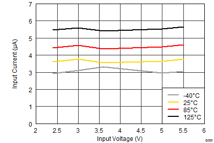
TPS62821 TPS62822 TPS62823 SLVSDV6_IQ.gif
Figure 1. Quiescent Current
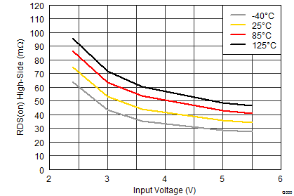
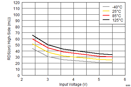
TPS62821 TPS62822 TPS62823 SLVSDV6_TPS62822_RDSON_HS.gif
Figure 3. High-Side Switch Resistance (TPS62821/2)
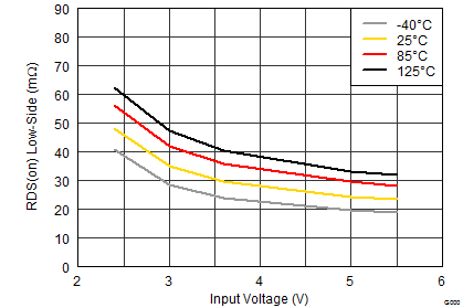
TPS62821 TPS62822 TPS62823 SLVSDV6_TPS62822_RDSON_LS.gif
Figure 5. Low-Side Switch Resistance (TPS62821/2/3)
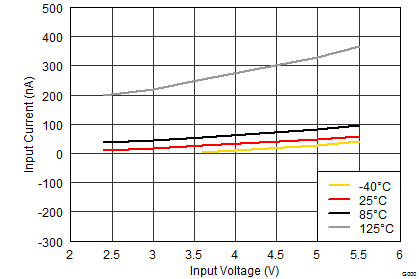
TPS62821 TPS62822 TPS62823 SLVSDV6_ISD.gif
Figure 2. Shutdown Current
TPS62821 TPS62822 TPS62823 SLVSDV6_TPS62823_RDSON_HS.gif
Figure 4. High-Side Switch Resistance (TPS62823)
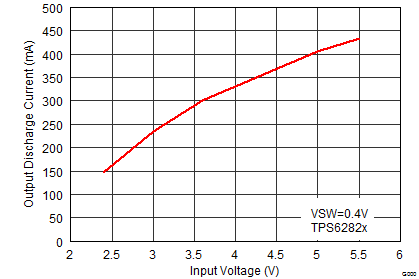
TPS62821 TPS62822 TPS62823 SLVSDV6_discharge_vin.gif
Figure 6. Active Output Discharge Current (EN=Low)