SLVSG04 November   2021 LM66200

PRODUCTION DATA  

  1. Features
  2. Applications
  3. Description
  4. Revision History
  5. Pin Configuration and Functions
  6. Specifications
    1. 6.1 Absolute Maximum Ratings
    2. 6.2 ESD Ratings
    3. 6.3 Recommended Operating Conditions
    4. 6.4 Thermal Information
    5. 6.5 Electrical Characteristics
    6. 6.6 Switching Characteristics
    7. 6.7 Typical Characteristics
  7. Detailed Description
    1. 7.1 Overview
    2. 7.2 Functional Block Diagram
    3. 7.3 Feature Description
      1. 7.3.1 Truth Table
      2. 7.3.2 Soft Start
      3. 7.3.3 Status Indication
    4. 7.4 VINx Collapse Rate
    5. 7.5 Output Voltage Drop
    6. 7.6 Device Functional Modes
      1. 7.6.1 Automatic Switchover
  8. Application and Implementation
    1. 8.1 Application Information
    2. 8.2 Typical Application
      1. 8.2.1 Design Requirements
      2. 8.2.2 Detailed Design Procedure
      3. 8.2.3 Application Performance Plots
  9. Power Supply Recommendations
  10. 10Layout
    1. 10.1 Layout Guidelines
    2. 10.2 Layout Example
  11. 11Device and Documentation Support
    1. 11.1 Documentation Support
      1. 11.1.1 Related Documentation
    2. 11.2 Receiving Notification of Documentation Updates
    3. 11.3 Trademarks
    4. 11.4 Electrostatic Discharge Caution
    5. 11.5 Glossary
  12. 12Mechanical, Packaging, and Orderable Information

Application Performance Plots

The below oscilloscope capture shows 5 V being applied to VIN1. The output comes up with slew rate control and limits the inrush current to below 500 mA.
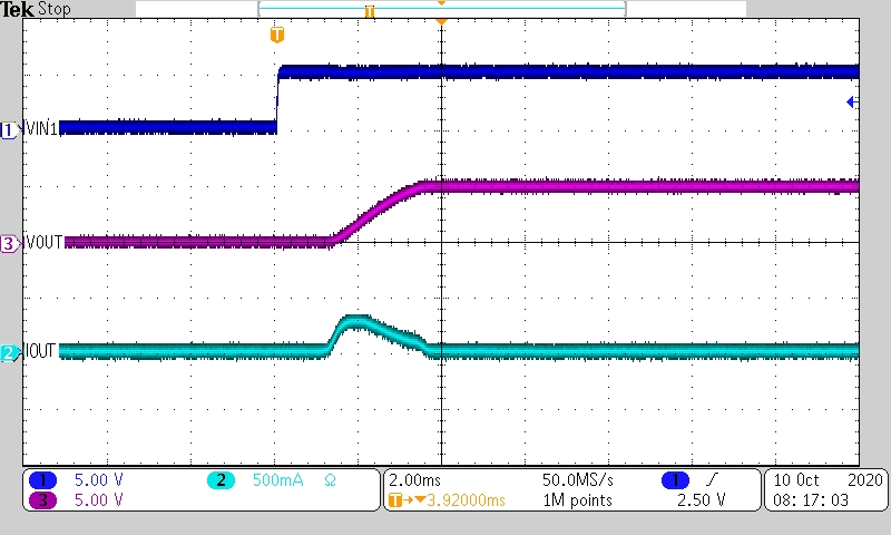
GUID-20210108-CA0I-MRBG-9DFB-QCCZHRDT3JR4-low.jpgFigure 8-2 LM66200 Inrush Current Control