SLVSG04 November   2021 LM66200

PRODUCTION DATA  

  1. Features
  2. Applications
  3. Description
  4. Revision History
  5. Pin Configuration and Functions
  6. Specifications
    1. 6.1 Absolute Maximum Ratings
    2. 6.2 ESD Ratings
    3. 6.3 Recommended Operating Conditions
    4. 6.4 Thermal Information
    5. 6.5 Electrical Characteristics
    6. 6.6 Switching Characteristics
    7. 6.7 Typical Characteristics
  7. Detailed Description
    1. 7.1 Overview
    2. 7.2 Functional Block Diagram
    3. 7.3 Feature Description
      1. 7.3.1 Truth Table
      2. 7.3.2 Soft Start
      3. 7.3.3 Status Indication
    4. 7.4 VINx Collapse Rate
    5. 7.5 Output Voltage Drop
    6. 7.6 Device Functional Modes
      1. 7.6.1 Automatic Switchover
  8. Application and Implementation
    1. 8.1 Application Information
    2. 8.2 Typical Application
      1. 8.2.1 Design Requirements
      2. 8.2.2 Detailed Design Procedure
      3. 8.2.3 Application Performance Plots
  9. Power Supply Recommendations
  10. 10Layout
    1. 10.1 Layout Guidelines
    2. 10.2 Layout Example
  11. 11Device and Documentation Support
    1. 11.1 Documentation Support
      1. 11.1.1 Related Documentation
    2. 11.2 Receiving Notification of Documentation Updates
    3. 11.3 Trademarks
    4. 11.4 Electrostatic Discharge Caution
    5. 11.5 Glossary
  12. 12Mechanical, Packaging, and Orderable Information

Automatic Switchover

When both inputs are applied to the device, the highest voltage is used to power the output. IThe ON pin is used as an active low device enable, turning off the device when it is pulled high. When the device is turned back on, soft start is used to power the output. The expected behavior for the device is shown in the waveform below.
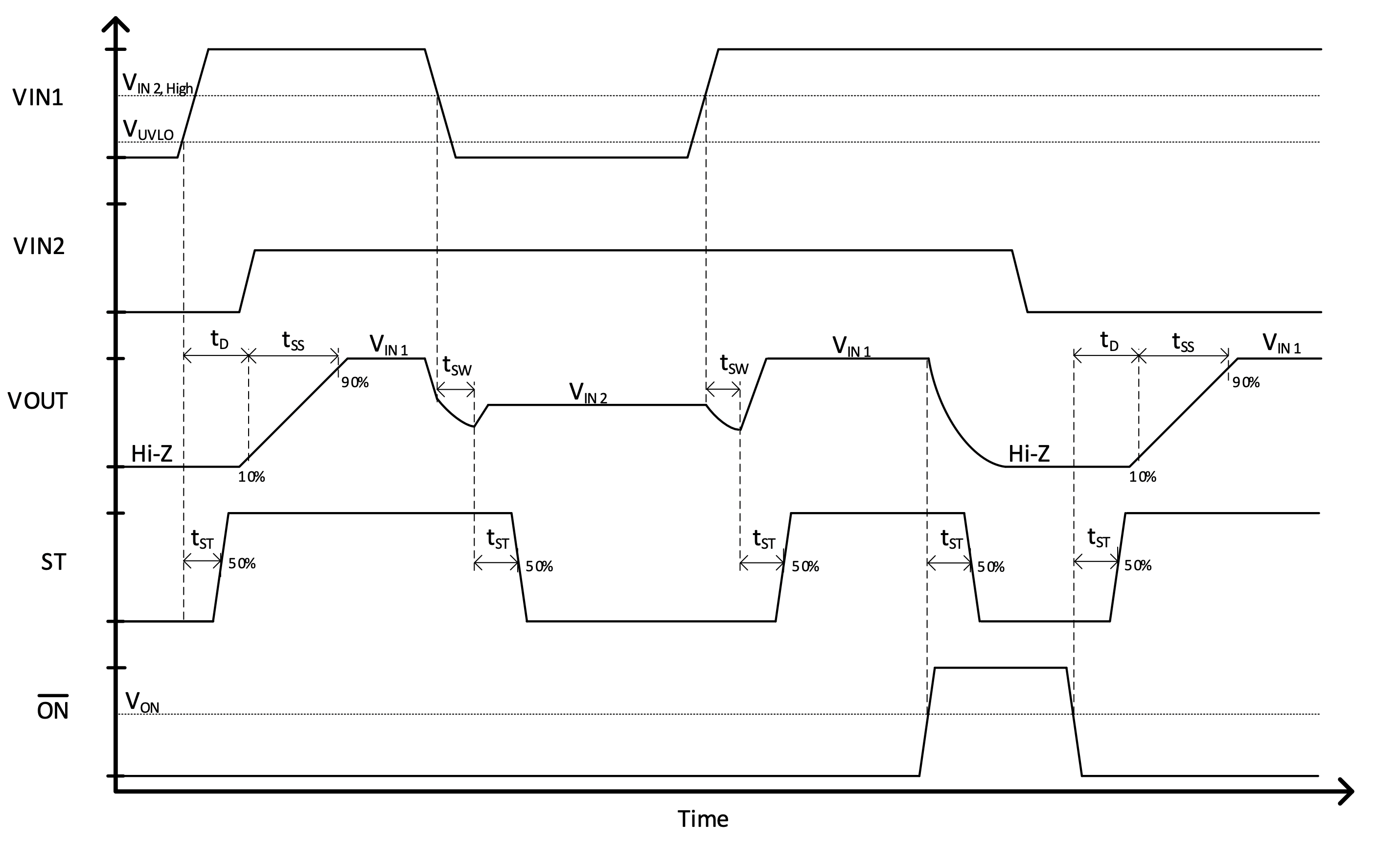
GUID-20211101-SS0I-MSG8-T887-7KXCJ0XSVGGS-low.pngFigure 7-1 Automatic Switchover Waveform